Voltage Lockdown: Investigating AMD's Recent AM5 AGESA Updates on ASRock's X670E Taichi
by Gavin Bonshor on May 16, 2023 12:00 PM EST- Posted in
- CPUs
- AMD
- ASRock
- Motherboards
- X3D
- Ryzen 7000
- X670E Taichi
- AGESA
AGESA 1.0.0.5c to 1.0.0.7: Differences With ASRock's X670E Taichi Firmware
Before we head into the testing, we figured it would be a good idea to highlight what we found different (if anything) within the BIOS of ASRock's X670E Taichi motherboard when updating the firmware from each successive version. Although nothing has changed from a GUI perspective, we can at least see some of the main settings that ASRock is presetting once AMD's EXPO memory profiles are enabled.
Screenshot of ASRock X670E Taichi UEFI firmware: BIOS 1.18 (AGESA 1.0.0.5c)
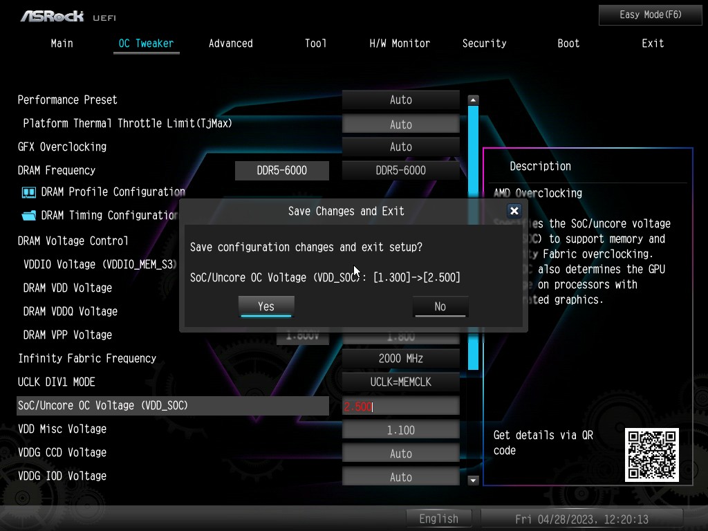
While nothing has changed in regards to the GUI, the most significant change from going from AMD's initial Ryzen 7000X3D-enabled BIOS is that users were able to set crazy levels of SoC voltage; the X670E Taichi would let us put 2.50 V on the SoC, which is ridiculously dangerous. As a reminder, the Ryzen 7000X3D chips are non-overclockable from a core frequency and VCore perspective, though they do support AMD EXPO memory profiles.
ASRock is clearly overshooting SoC voltage to ensure stability for users. When applying AMD EXPO on supported DRAM, all of ASRock's X670E Taichi firmware variants from AGESA 1.0.0.5c to the latest BETA AGESA 1.0.0.7 (BETA) variant, the firmware would automatically apply 1.30 V to the SoC voltage, regardless of what memory frequency is used. If users opt for a lower spec kit such as DDR5-6000 with EXPO, applying 1.30 V is a little overkill, as we found it made no difference to stability until we went below 1.25 V on the SoC voltage.
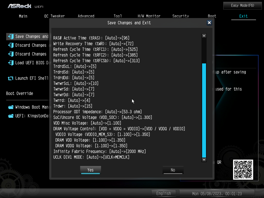
ASRock X670E Taichi firmware applying changes when using EXPO on our DDR5-6000 EXPO kit.
Looking at the changes that applying memory with an AMD EXPO profile has on the settings, we can see that ASRock automatically changes some key voltage settings relating to SoC, VDDIO, DRAM VDD, and DRAM VDDQ. As we previously mentioned, ASRock automatically applies 1.30 V to the SoC voltage when you use EXPO memory profiles, or even XMP 3.0 profiles, as we found out. The VDD misc voltage was set to 1.10 V from auto, with the DRAM voltage (DRAM VDD/VDDQ) increasing to 1.350 V from 1.10 V. As per the memory specifications and how AMD's Infinity Fabric works, the firmware automatically applied 2000 MHz for Infinity Fabric and changed the UCLK DIV from auto to equal the MEMCLK.
AMD AGESA 1.0.0.5c Up to 1.0.0.7: Analysis, Testing For Differentials
For our analysis of the changes that AMD's updated AGESA firmware has on specific variables when put under heavy and intensive memory-focused workloads, we'll be splitting the sections into two; memory at the JEDEC default specifications (settings on auto) and with EXPO enabled (DDR5-6000 CL34).
G.Skill Trident Z5 at DDR5-5200 (JEDEC) Settings
The key variables we'll be focusing on include the following:
- Peak Temperatures across the CPU die, CPU CCD1 (3D V-Cache), and CPU CCD2 (in °C)
- Peak Voltages including CPU VDDCR/VDD, CPU VDDR_SoC (SoC Voltage)
- Peak Current, including CPU Core current and SoC current (in amps)
- Peak Power, including CPU PPT (from the AM5 socket) and SoC power
In our results, the CPU die temp max average is an average of both CCD1, CCD2, core temperatures and L3 cache temperatures. This isn't to be confused with the average of the CPU die temp average.
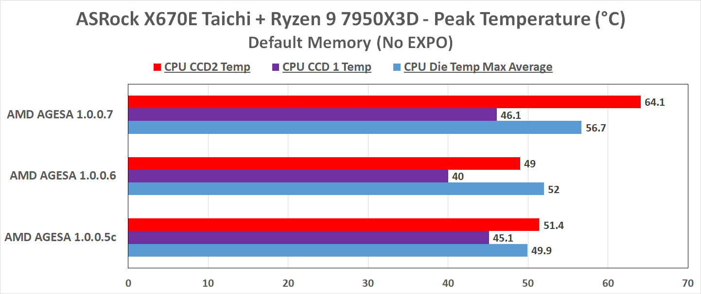
Starting with peak temperatures across both CCDs and the die, going from AGESA 1.0.0.5c to AGESA 1.0.0.7 (BETA), we can see that the CCD2 (non-V-Cache) was noticeably higher by just under 25%. The CCD (1) with 3D V-Cache was relatively consistent regarding peak temperatures, with a jump of just 2%. Overall, the CPU die temp, as with CCD1, was higher due to the different core temperatures on CCD2.
We can see that going to AGESA 1.0.0.6 from 1.0.0.5c resulted in slightly lower temperatures across all of the CCDs and overall die temp, but the latest AGESA 1.0.0.7 (BETA) (at the time of writing) was the hottest of all. One possible reason for the higher temperatures on AGESA 1.0.0.7 is that reducing power from the one component of the CPU, in this case, the SoC allows the actual Zen 4 cores slightly more headroom in terms of power.
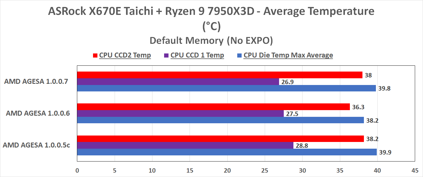
Looking at the average temperatures across CCD1 and CCD2 and the overall die temperature, we can see that there wasn't much variance between the different AGESA versions. Even on AGESA 1.0.0.7 with a higher temperature peak, the average is much more in line with the other AGESA versions.
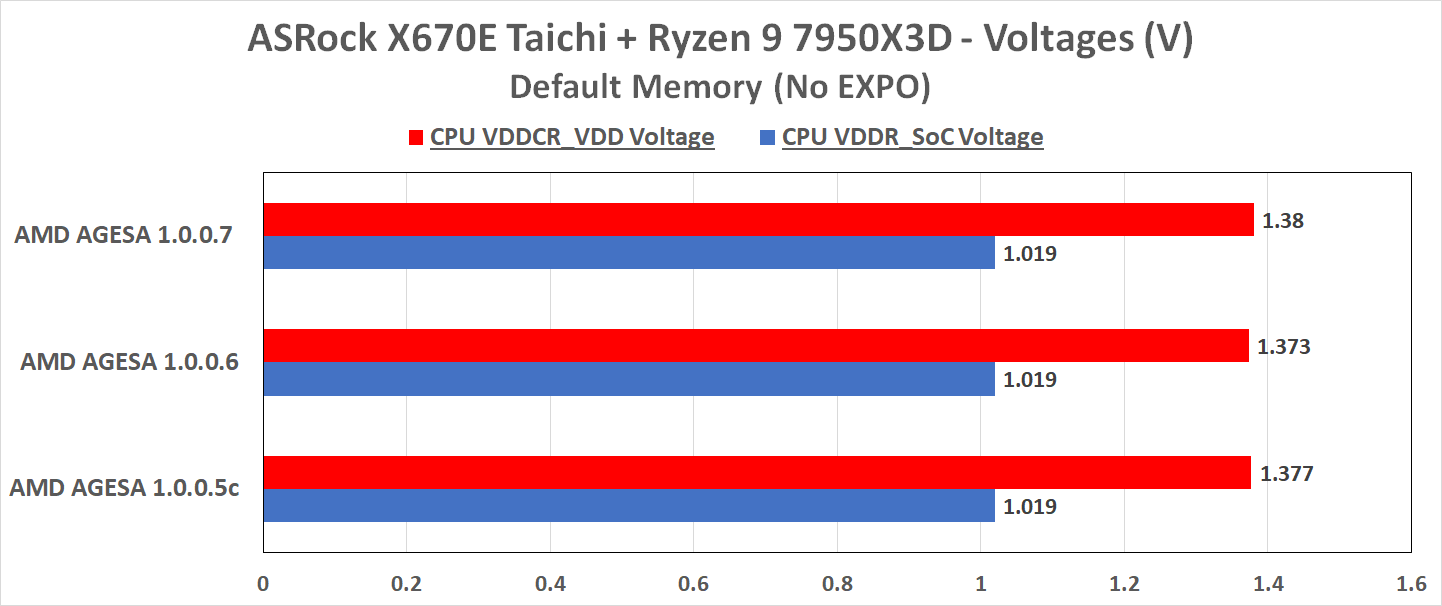
Focusing on voltages, including CPU VDDCR_VDD (memory voltage) and CPU VDDR_SoC voltages, we can see they are consistently within acceptable margins. While we're not focused on CPU VCore as it's well within specification, and hasn't been an issue as the Ryzen 7000X3D series chips are core frequency/voltage locked, the SoC and memory voltages are well within expected levels in line with our G.Skill Trident Z5 Neo DDR5-6000 memory's specifications.
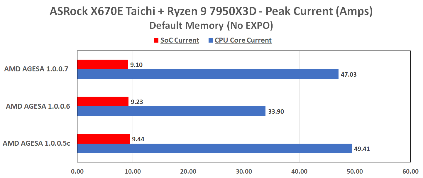
Although we observed higher temperatures across the board on AGESA 1.0.0.7 (BETA) without AMD's EXPO enabled, we can see that AGESA 1.0.0.5c's current peaked higher. While sustained current and voltages can spike higher than the averages, they aren't sustained and shouldn't be of concern, at least not from our testing.
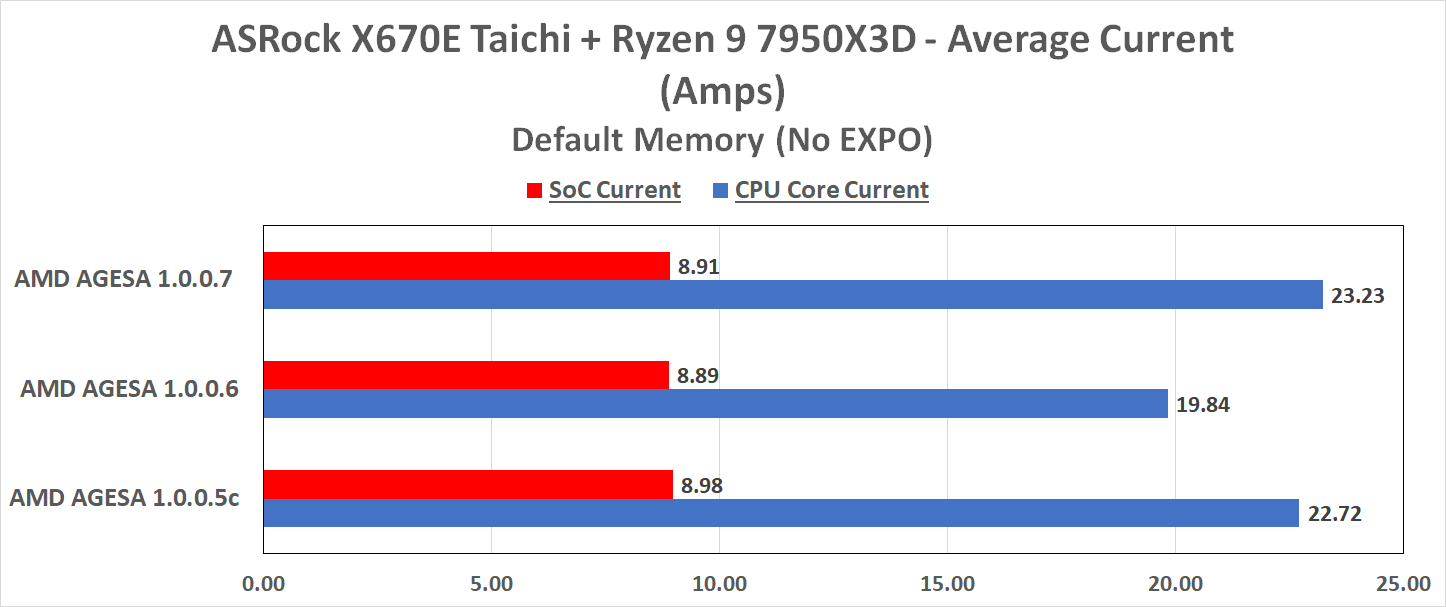
Focusing on the averages of both the SoC and CPU Core currents, we can see that AGESA 1.0.0.6 is slightly more reserved than the initial Ryzen 7000X3D series launch firmware and the latest AGESA 1.0.0.7 (BETA).
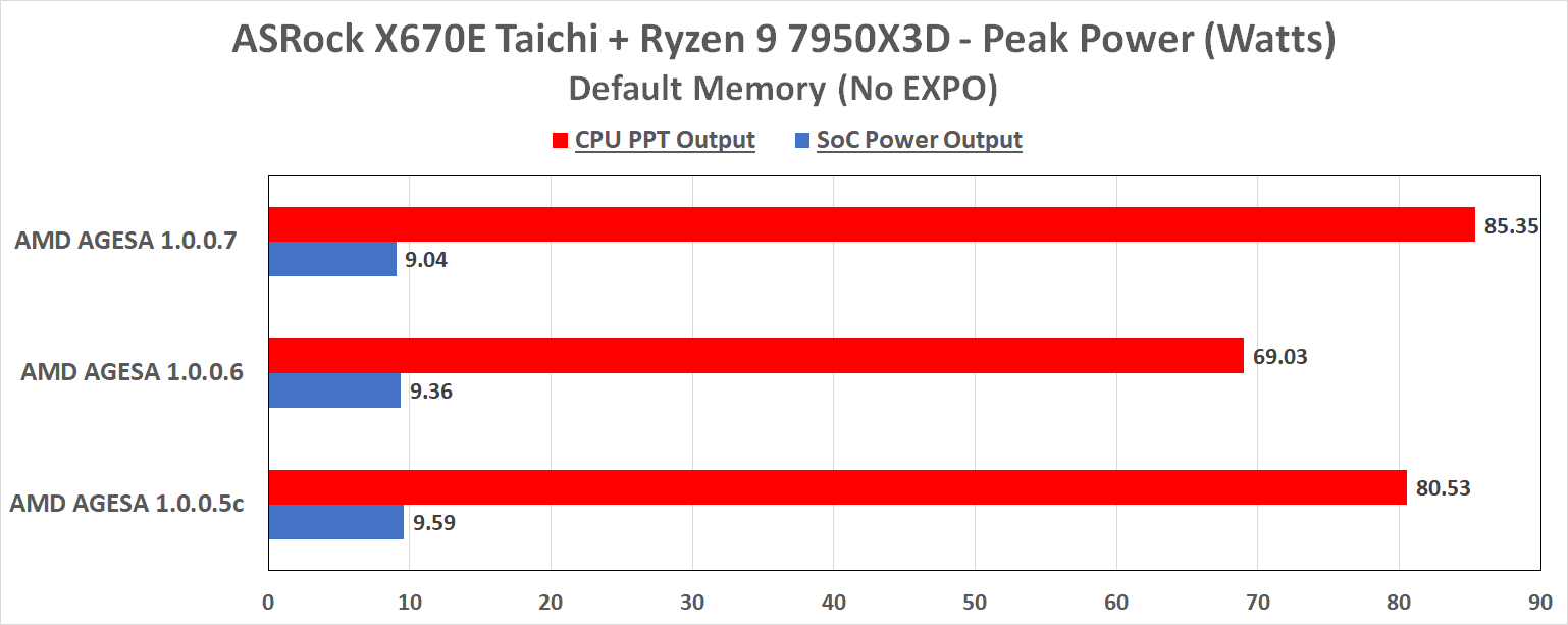
The actual power values monitored using HWInfo show that AGESA 1.0.0.7 (BETA) has a higher peak power from the socket (PPT) than the two other AGESA versions. As we've seen from our testing, AGESA 1.0.0.6 with our ASRock X670E Taichi is more conservative on current and power, so temperatures are lower across the board. Pulling more power from the socket with AGESA 1.0.0.7 (BETA) and our Ryzen 9 7950X3D does explain why temperatures are higher, both at peak and average.
Our testing shows that AMD's AGESA 1.0.0.7 (BETA) is consistent with other AGESA firmware versions at default memory settings. Still, we can see an increase in power draw and temperatures, at least on the ASRock X670E Taichi.
G.Skill Trident Z5 at DDR5-6000 (EXPO Enabled) Settings
Now onto our testing with the AMD EXPO memory profile enabled on our G.Skill Trident Z5 Neo DDR5-6000 CL34 kit. We've added another variable, with our DDR5-6000 kit also running with an applied SoC voltage of 1.25 V in the firmware.
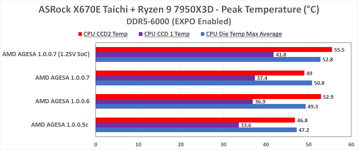
A closer look at peak temperatures shows a slight variation between all three AGESA firmware variants. Using AMD AGESA 1.0.0.7 (BETA) with 1.25V on the SoC voltage, CCD2 peaked at 55.5°C, the CCD without the 3D V-Cache. This was a noticeably higher spike than expected, given that SoC voltage was inherently lower than the other runs (1.30 V on the SoC).
Interestingly, the initial launch BIOS (AGESA 1.0.0.5c) for Ryzen 7000X3D processors ran with the lowest temperature on CCD2, and we observed the lowest spike in temps on CCD1 (3D V-Cache) too. Looking at the maximum CPU die temperature average, all were within quite acceptable margins, with nothing noteworthy in this regard and nothing out of the ordinary.
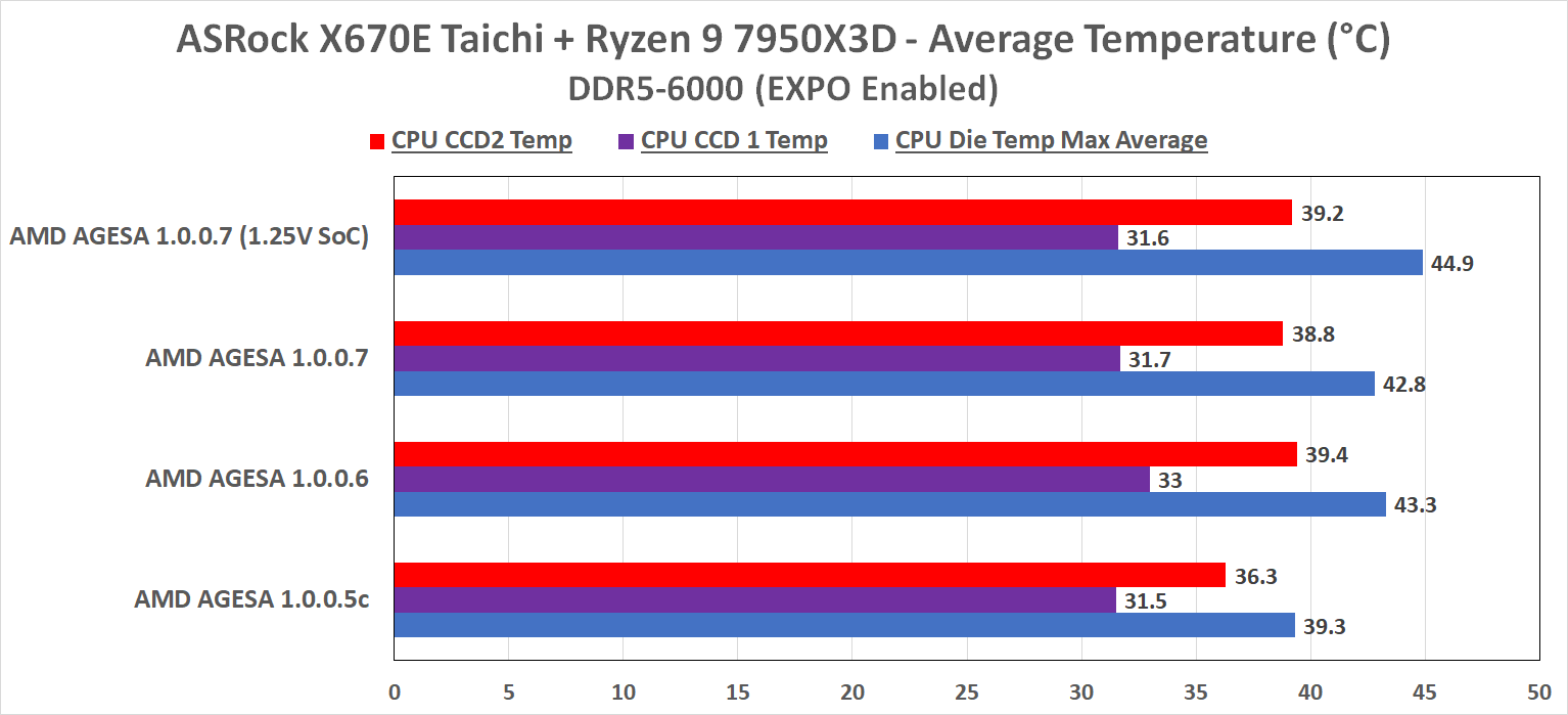
Moving to the average temperatures, we see things are much more balanced between the three AMD AGESA firmware versions. AGESA 1.0.0.7 (BETA) at 1.25 V on the SoC voltage still averaged slightly warmer on the non-3D V-Cache enabled CCD than on AGESA 1.0.0.5c, which was less on average compared to AGESA 1.0.0.6.
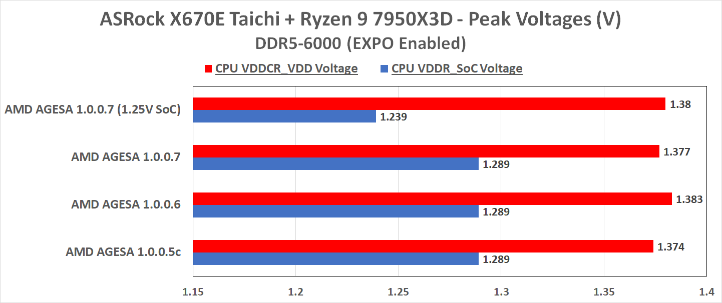
Concentrating on peak voltages across both the memory and CPU SoC voltages, we can see that AMD AGESA 1.0.0.6 peaked slightly higher on memory voltage than the other revisions. SoC voltage is consistent across all three AGESA variants at 1.289, showing that ASRock's firmware automatically setting 1.30 V for SoC is working well. At 1.25 V on AGESA 1.0.0.7 (BETA), our SoC voltage reading topped out at 1.239 V, which shows a bit of negative VDroop, a positive in this case.
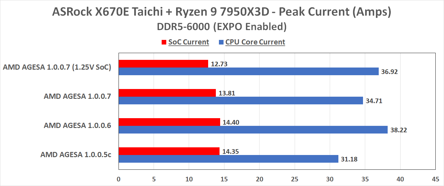
Again, AGESA 1.0.0.6 is operating with more courage as it pulls more amps than other versions; it's interestingly peaking at a higher current on the SoC voltage than the firmware before it, AGESA 1.0.0.6. It would have been thought that AMD's quick fix BIOS to address SoC voltages would peak at lower variables, and it peaks around half an amp higher than the latest AGESA 1.0.0.7 (BETA) firmware.
Even setting 1.25 V on the SoC, the amperage pulled from the rail responsible for the SoC is lower than 1.30 V, which is expected as less power is fed through it. Although we didn't experience any reported problems in our testing, CPU core current spiked higher on AGESA 1.0.0.6 than the other versions.
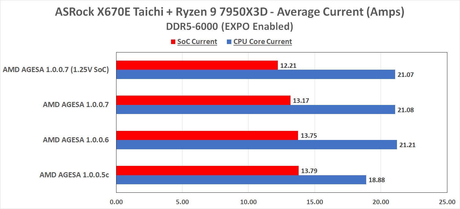
Focusing on average amps drawn from the SoC, things on the SoC balance back to expected levels, although there is not much variation comparing all three AGESA firmware. On average, with AGESA 1.0.0.6 and 1.0.0.7, we can see that the average CPU core current is noticeably higher than AGESA 1.0.0.5c, which is the initial launch BIOS for the X670E Taichi for Ryzen's 7000X3D series.
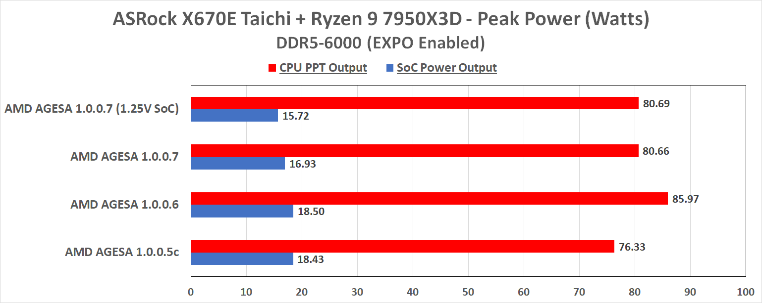
Lastly, the peak power output with AMD's EXPO memory profile enabled on our Ryzen 9 7950X3D with the ASRock X670E Taichi. As we can see, AMD AGESA 1.0.0.6 peaked out over 5 W higher on the AM5 socket than the other versions, and AGESA 1.0.0.5c seems to be the most conservative regarding this. For SoC power output, AGESA 1.0.0.6 spikes higher on power than the different versions, which could be one of the reasons that AMD replaced AGESA 1.0.0.6 so quickly.


39 Comments
View All Comments
techjunkie123 - Tuesday, May 16, 2023 - link
Any by anandtech reviewer, I meant reader.TheinsanegamerN - Wednesday, May 17, 2023 - link
As predicted, GN calls out AMD and people start whining.Silver5urfer - Wednesday, May 17, 2023 - link
GN kisses Nvidia and people shrug off. Also their new Muh Failure rate website page, it does not list the LGA1700 socket engineering failure, but has 12VHPWR as "Fixed per GN standards" is laughable at best as the socket design causes other unwanted behavior along with the HS contact and longevity of the PCB traces. See Buildzoid IMC video on RPL, in short contact issue for the Socket but hey you can use the Thermalgrizzly Contact Frame and fix it while screwing your mobo in the process with non-factory Torque spec funnily Thermalright one is far superior, however since GN said the former is good all people learn the hardway.Both the OPs are correct, throwing a bunch of zoom images and extrapolating on lack of information with confusing the end user tricking onto some space age analysis does not help. Meanwhile AT's solid pieces on both LGA1700 bendgate and the AGESA on X3D provides far more useful information the Thermal and Electrical behavior from 3 diff AGESA versions is excellent approach to check what is going on than poking in the dark (Lithography, Metallurgy etc), only positive thing to come out of GN was ASUS rolling back their shady tactics esp many YTers called them out.
Anandtech has no rival in how they cover, I wish they reviewed GPUs and staff did not leave (Ian, Andrei etc), but the facts are hard truth, like the YT content killed blogs like this which is a big loss to many but most of the people around the world do not care for in-depth pieces and real Tech Journalism which is not capitalizing on the content for clicks. All the reviewers out there just simply copy paste the slide deck OR read their PR guide in virtually all the sites / videos except AT.
cheshirster - Tuesday, May 16, 2023 - link
"we can see that everything is fundamentally well within control"I've seen an interesting behavior on GB board.
It was trying to prevent high voltage delta between vmem and vsoc when using manual settings.
The parasite current between different voltage lines (in case of too big delta) could be the case of the problem and you won't see the solution working by simply measuring voltages.
meacupla - Tuesday, May 16, 2023 - link
On Ryzen 2000, 3000, and 5000, high voltage delta between Vsoc and Vram did result in poor ram stability. Particularly when the DDR4 required more than 1.35V to run at its rated speed.Silver5urfer - Tuesday, May 16, 2023 - link
I already knew that Failure Analysis Lab won't do anything. It is known fact that how can an unnamed lab can breakdown the reason of the CPU failure after the fact when they are not the ones associated with the OEM manufacturer of the said processor. Same for that 12VHPWR GN's video which did not yield anything. It's just a shock value capitalization for the maximum hits on the topic the real deal was 12VHPWR Nvidia statement which was given to GN rather like AMD who is giving it from their PR handle directly, allowing Nvidia to shrug off.Anyways moving on the AMD perhaps did not do proper verification as this is their First take at EXPO and the Zen 4 processor outside the Server HPC space where they are severely limited to add the extra consumer features like Overclocking, and Intel has an edge here because Intel has been doing the OC business since their Core series processors debuted on DDR3 which means literally 2-3 generations of Memory Overclock experience. Plus they sponsor HWBot too.
I find Anandtech's conclusions far more useful, yet read non conclusive as stated which is obvious when you are dealing with Microprocessors made in this era where we have ton of variables at play. Plus gives a good insight on how the Current, Voltage and Temperatures are being effected thus giving some picture of the inner workings of the CPU which we cannot really ever know because one AMD does not provide documentation / datasheets like Intel, two is these are bleeding edge tech, it's hard to know many things esp when you have a non monolithic design, on Intel it's easy and esp Intel can fix the clock rate as in user can do it. Plus no uncore sitting on a different piece of die (may change in MTL and ARL in the future).
So yea this is a great piece on how the AGESA varies than a nice Electron Microscope zoom picture content with a ton of VLSI terminology thrown at the user to confuse them. However I do agree with GN's ASUS part 100%, because that company has been complete pile of rubbish nowadays. I had to return a lot of Z590 boards because their Mobo PCB paint was chipped off on brand new APEX boards. Then the whole BIOS problems associated with ASUS - ROG Forums are a disaster now, they killed the site with mobile focus. ASUS implements ARB, Anti Roll Back, forcing you to get restricted to a BIOS this is very bad because on Z590 their boards had RTX40 series PCIe4.0 issue as in they did not run on 4.0 speed. Beta BIOS had the fix but actual update did not and they had ARB on the actual one, that's how bad ASUS is, some of them cannot even be rolled back even if you use BIOS Flashback. The Armory Crate is a cancer software which you cannot get rid of due to Registry into deep OS stack. Same like Intel XTU (Should use Throttlestop which is leagues ahead).
All in all it's unfortunate situation AMD should improve this and gain from this experience, they learned a lot with Zen 3, the IODie was a mess on it now Zen 4 is solid in that dept esp when they reduced the Memory variables from 3 values (fclk, mclk, uclk) in zen 3 to zen 4 now only has 2 resulting in a stable I/O handling. Plus the significantly higher clock ratio etc.
Silver5urfer - Tuesday, May 16, 2023 - link
More clarification,Nvidia's 12VHPWR ultimately was flawed as Intel ATX 3.0 power revises the 4 Sense pins to be elongated plus use of the Tulip design vs the Dot which was mentioned by Igor and ignored by GN. And the fact that AMD's R9 295 X2 on Anandtech here pulls 500W using just 2x8Pin standard further reinforcing that 12VHPWR is a clearly rushed one, and the fact that RTX 3090Ti does not have this problem because of lack of 4 Sense pins thus limiting the hard power cap.
And about ASUS, to add after getting caught they are now issuing a PR that all Mobos with EXPO and Beta also are covered under warranty. GN take did something good they have a long way to go esp how their BIOS is top notch yet they cram too much voltage into every possible way. Taking advantage of the brand value and consumer mindset.
Hairs - Saturday, May 27, 2023 - link
Igor's analysis on the 12vHPWR was absolute guesswork based on looking at some mobile phone pictures posted to reddit.The failure analysis lab pointed out that tulip vs dot would not provide sufficient difference in power connector stability to cause the issue on its own, as suggested by Igor.
GN is the only tech outlet that did any actual testing on the cables, and they did this not just by sending one out to a professional lab for verification, but by doing individual unit tests on multiple physical tables to re-create possible error scenarios. Of all the possiblities (and they tested different cables from different vendors) the only one which reliably recreates the burnout is when the connector is both not fully seated, and also sits at a slight angle in the socket. Both of these are user-error problems, but the user error is compounded by the fact that the physical security of the socket (not the internal design of the pin connectors) isn't robust enough compared to the old 8-pin design.
Literally everyone else was guessing. Only GN actually tried to recreate the problem and validate what was going on.
Hairs - Saturday, May 27, 2023 - link
"The key takeaway is that, at least on the ASRock X670E Taichi, things are working as they should be with AGESA 1.0.0.7 (BETA), and we look forward to a full release (non-BETA) of their latest AGESA in the coming weeks."Anandtech haven't event tested OCP, which is one of ASUS's primary failures and yet claim "everything" is working. Great conclusion and in-depth analysis there. "Ignore that other reviewer who claims there are multiple problems, I ran HWinfo and it's grand."
Calling GN's work "shock value capitalization" when they were literally the only tech reviewers either on YT or on written blogs who took actual time to analyse things and delayed their content specifically to avoid bandwagon-jumping and pushing a scare narrative that all cards using the connector were guaranteed to burn up is laughable.
Where was Anandtech's deep analysis of the topic? Oh right they haven't done any GPU work in years other than reprint PR releases.
army165 - Tuesday, May 16, 2023 - link
I have a 7800X3D and an Asus B650 board. Should I take it out and inspect it for damage? I upgraded to the 1303 BIOS when I got the board and didn't move to the Beta BIOS 1410 until after Asus redacted their "we won't fix this if you use this" message on the BIOS description.