AMD Zen 4 Ryzen 9 7950X and Ryzen 5 7600X Review: Retaking The High-End
by Ryan Smith & Gavin Bonshor on September 26, 2022 9:00 AM ESTZen 4 Execution Pipeline: Familiar Pipes With More Caching
Finally, let’s take a look at the Zen 4 microarchitecture’s execution flow in-depth. As we noted before, AMD is seeing a 13% IPC improvement over Zen 3. So how did they do it?
Throughout the Zen 4 architecture, there is not any single radical change. Zen 4 does make a few notable changes, but the basics of the instruction flow are unchanged, especially on the back-end execution pipelines. Rather, many (if not most) of the IPC improvements in Zen 4 come from improving cache and buffer sizes in some respect.
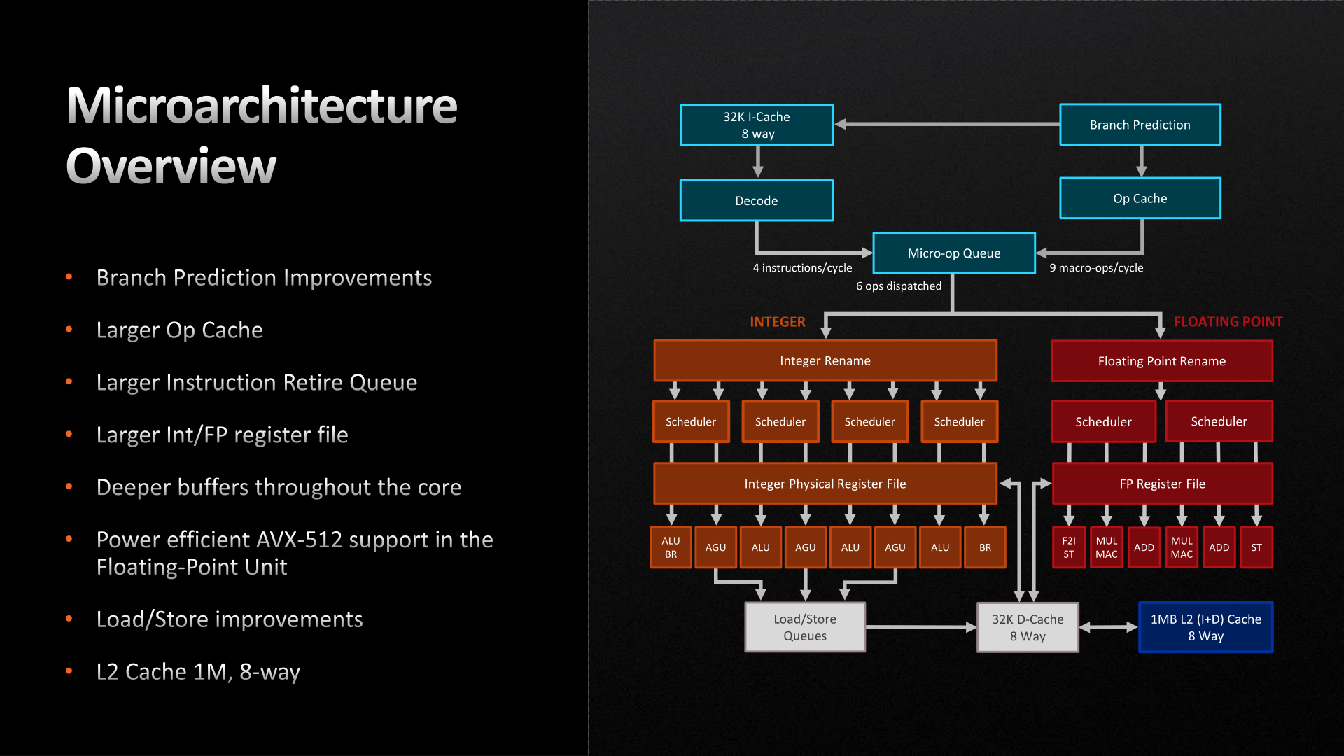
Starting with the front end, AMD has made a few important improvements here. The branch predictor, a common target for improvements given the payoffs of correct predictions, has been further iterated upon for Zen 4. While still predicting 2 branches per cycle (the same as Zen 3), AMD has increased the L1 Branch Target Buffer (BTB) cache size by 50%, to 2 x 1.5k entries. And similarly, the L2 BTB has been increased to 2 x 7k entries (though this is just an ~8% capacity increase). The net result being that the branch predictor’s accuracy is improved by being able to look over a longer history of branch targets.
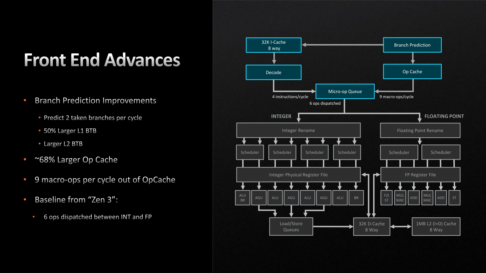
Meanwhile the branch predictor’s op cache has been more significantly improved. The op cache is not only 68% larger than before (now storing 6.75k ops), but it can now spit out up to 9 macro-ops per cycle, up from 6 on Zen 3. So in scenarios where the branch predictor is doing especially well at its job and the micro-op queue can consume additional instructions, it’s possible to get up to 50% more ops out of the op cache. Besides the performance improvement, this has a positive benefit to power efficiency since tapping cached ops requires a lot less power than decoding new ones.
With that said, the output of the micro-op queue itself has not changed. The final stage of the front-end can still only spit out 6 micro-ops per clock, so the improved op cache transfer rate is only particularly useful in scenarios where the micro-op queue would otherwise be running low on ops to dispatch.
Switching to the back-end of the Zen 4 execution pipeline, things are once again relatively unchanged. There are no pipeline or port changes to speak of; Zen 4 still can (only) schedule up to 10 Integer and 6 Floating Point operations per clock. Similarly, the fundamental floating point op latency rates remain unchanged as 3 cycles for FADD and FMUL, and 4 cycles for FMA.
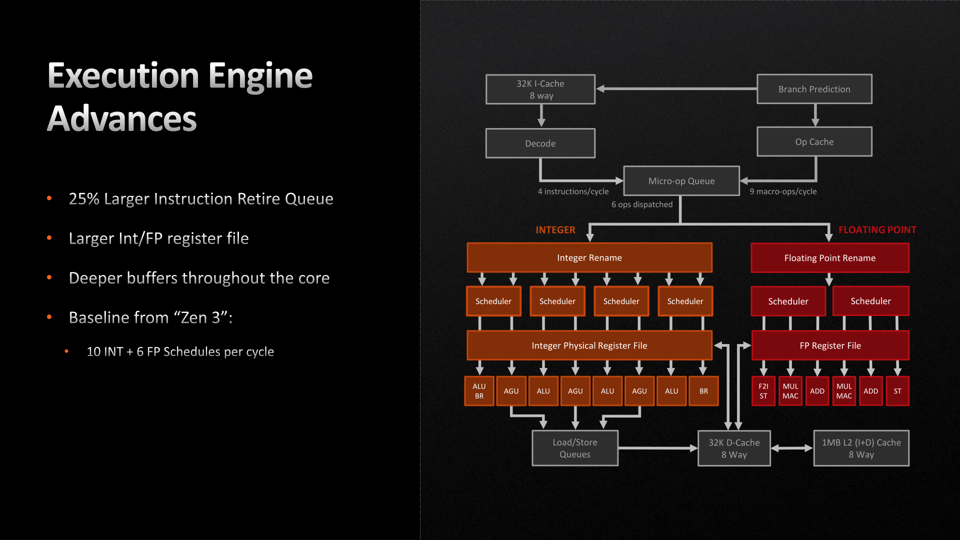
Instead, AMD’s improvements to the back-end of Zen 4 have here too focused on larger caches and buffers. Of note, the retire queue/reorder buffer is 25% larger, and is now 320 instructions deep, giving the CPU a wider window of instructions to look through to extract performance via out-of-order execution. Similarly, the Integer and FP register files have been increased in size by about 20% each, to 224 registers and 192 registers respectively, in order to accommodate the larger number of instructions that are now in flight.
The only other notable change here is AVX-512 support, which we touched upon earlier. AVX execution takes place in AMD’s floating point ports, and as such, those have been beefed up to support the new instructions.
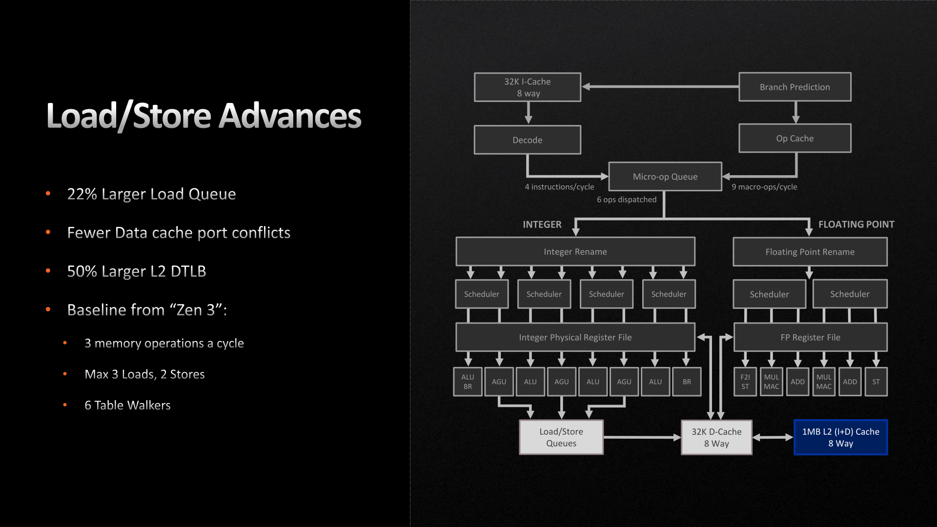
Moving on, the load/store units within each CPU core have also been given a buffer enlargement. The load queue is 22% deeper, now storing 88 loads. And according to AMD, they’ve made some unspecified changes to reduce port conflicts with their L1 data cache. Otherwise the load/store throughput remains unchanged at 3 loads and 2 stores per cycle.
Finally, let’s talk about AMD’s L2 cache. As previously disclosed by the company, the Zen 4 architecture is doubling the size of the L2 cache on each CPU core, taking it from 512KB to a full 1MB. As with AMD’s lower-level buffer improvements, the larger L2 cache is designed to further improve performance/IPC by keeping more relevant data closer to the CPU cores, as opposed to ending up in the L3 cache, or worse, main memory. Beyond that, the L3 cache remains unchanged at 32MB for an 8 core CCX, functioning as a victim cache for each CPU core’s L2 cache.
All told, we aren’t seeing very many major changes in the Zen 4 execution pipeline, and that’s okay. Increasing cache and buffer sizes is another tried and true way to improve the performance of an architecture by keeping an existing design filled and working more often, and that’s what AMD has opted to do for Zen 4. Especially coming in conjunction with the jump from TSMC 7nm to 5nm and the resulting increase in transistor budget, this is good way to put those additional transistors to good use while AMD works on a more significant overhaul to the Zen architecture for Zen 5.


205 Comments
View All Comments
Tomatotech - Friday, September 30, 2022 - link
Nice idea but you’re swimming against the flow of history. The trend is always to more tightly integrate various components into smaller and smaller packages. Apple have moved to onboard RAM in the same package as the CPU which has bought significant bandwidth advantages and seems to have boosted iGPU to the level of low-end dGPUs.The main takeaway from your metaphor of the 650w dGPU with a 55w mainboard and 100-200w CPU is that high-end dGPUs are now effectively separate computers in their own right - especially as a decent one can be well over 50% of the cost of the whole PC - and are being constrained by having to fit into the PC in terms of physical space, power supply capacity, and cooling capacity.
It’s a shrinking market on both the low end and high end for home use of dGPU, given these innovations and constraints and I don’t know where it’s going to go from here.
Since I got optic fibre, I’ve started renting cloud based high-end dGPU and it has been amazing albeit the software interface has been frustrating at times. With symmetric gigabit service and 1-3ms ping, it’s like having it under my desk. I worked out that for unlimited hours and given the cost of electricity, it would take 10 years for my cloud rental costs to match the cost of buying and running a home high end dGPU.
Not everyone has optic fibre of course but globally it’s rolling out year by year so the trend is clear again. Reply
Castillan - Wednesday, September 28, 2022 - link
"clang version 10.0.0
clang version 7.0.1 (ssh://git@github.com/flang-compiler/flang-driver.git
24bd54da5c41af04838bbe7b68f830840d47fc03)
-Ofast -fomit-frame-pointer
-march=x86-64
-mtune=core-avx2
-mfma -mavx -mavx2
"
...and then later the article says:
"The performance increase can be explained by a number of variables, including the switch from DDR4 to DDR5 memory, a large increase in clock speed, as well as the inclusion of the AVX-512 instruction set, albeit using two 256-bit pumps."
The problem here being that those arguments to Clang will NOT enable AVX-512. Only AVX2 will be enabled. I verified this on an AVX512 system.
To enable AVX512, at least at the most basic level, you'll want to use "-mavx512f ". There's also a whole stack of other AVX512 capabilities, which are enabled with "-mavx512dq -mavx512bw -mavx512vbmi -mavx512vbmi2 -mavx512vl" but some may not be supported. It won't hurt to include those on the command line though, until you try to compile something that makes use of those specific features, and then you'll see a failure if the platform doesn't support those extensions. Reply
Ryan Smith - Friday, September 30, 2022 - link
Correct. AVX-512 is not in play here. That is an error in analysis on our part. Thanks! Replypman6 - Thursday, September 29, 2022 - link
intel supports 8k60 AV1 decode.Does ryzen 7000 support 8k60 ?? Reply
GeoffreyA - Monday, October 3, 2022 - link
The Radeon Technology Group is getting 16K ready. Replyyhselp - Thursday, September 29, 2022 - link
I'd love to see you investigate memory scaling on the Zen 4 core. ReplyMyrandex - Thursday, September 29, 2022 - link
The table on page four mentions "Quad Channel (128-bit bus)" for memory support. Does that mean we could have a 4 memory slot solution, with one memory module per channel, with four channel support? This way to drastically increase memory bandwidth all while maintaining those fast DDR5 frequencies? ReplyRyan Smith - Friday, September 30, 2022 - link
No. That configuration would be no different than a 2 DIMM setup in terms of bandwidth or capacity. Slotted memory is all configured DIMMs; as in Dual Inline Memory Module. ReplyGeoffreyA - Friday, September 30, 2022 - link
All in all, excellent work, AMD, on the 7950X. Undoubtedly shocking performance. Even that dubious AVX-512 benchmark where Intel used to win, Zen 4 has taken command of it. However, lower your prices, AMD, and don't be so greedy. Little by little, you are becoming Intel. Don't be evil.Thanks, Ryan and Gavin, for the review and all the hard work. Much appreciated. Have a great week. Reply
Footman36 - Friday, September 30, 2022 - link
Yawn. I really don't see what the big fuss is about. I currently run 5600X and was interested to see how the 7600X compared and while it does look like a true uplift in performance over the 5600X, I would have to factor in cost of new motherboard and DDR5 ram! On top of that, the comparison is not exactly apples to apples in the testing. 7600X has a turbo speed of 5.3, 5600X 4.6. 7600X runs with 5200 DDR5 and 5600X 3200 DDR4, 7600X has TDP 105W, 5600X 65W. If you take a look at the final page where the 7950X is tested in ECO mode which effectively supplies 65W instead of 105W you lose 18% performance. If we try to do apples to apples and use eco mode with 7600X, to get apples to apples with 65W of 5600W, then lower boost to 4.6ghz then the performance of the 2 cpu's looks very similar. Perhaps not the way I should be analyzing the results, but just my observation.... Reply