AMD Zen 4 Ryzen 9 7950X and Ryzen 5 7600X Review: Retaking The High-End
by Ryan Smith & Gavin Bonshor on September 26, 2022 9:00 AM ESTZen 4 Execution Pipeline: Familiar Pipes With More Caching
Finally, let’s take a look at the Zen 4 microarchitecture’s execution flow in-depth. As we noted before, AMD is seeing a 13% IPC improvement over Zen 3. So how did they do it?
Throughout the Zen 4 architecture, there is not any single radical change. Zen 4 does make a few notable changes, but the basics of the instruction flow are unchanged, especially on the back-end execution pipelines. Rather, many (if not most) of the IPC improvements in Zen 4 come from improving cache and buffer sizes in some respect.
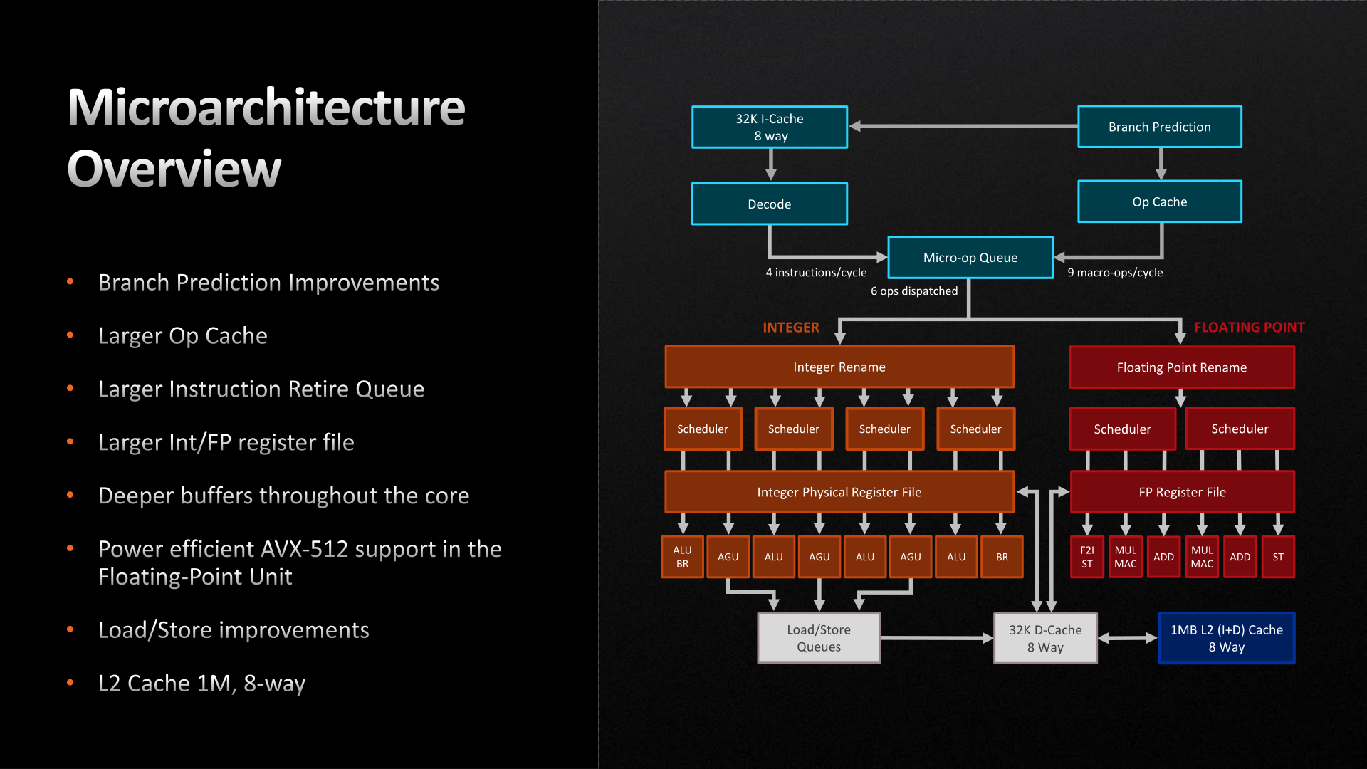
Starting with the front end, AMD has made a few important improvements here. The branch predictor, a common target for improvements given the payoffs of correct predictions, has been further iterated upon for Zen 4. While still predicting 2 branches per cycle (the same as Zen 3), AMD has increased the L1 Branch Target Buffer (BTB) cache size by 50%, to 2 x 1.5k entries. And similarly, the L2 BTB has been increased to 2 x 7k entries (though this is just an ~8% capacity increase). The net result being that the branch predictor’s accuracy is improved by being able to look over a longer history of branch targets.
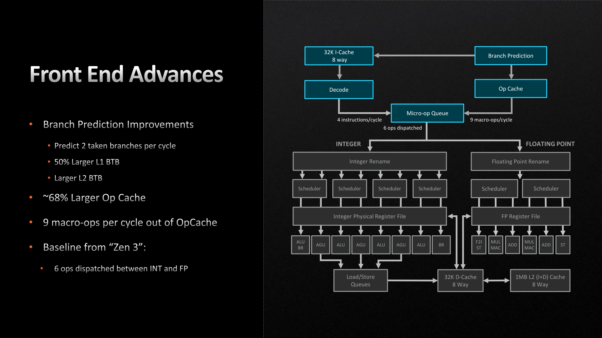
Meanwhile the branch predictor’s op cache has been more significantly improved. The op cache is not only 68% larger than before (now storing 6.75k ops), but it can now spit out up to 9 macro-ops per cycle, up from 6 on Zen 3. So in scenarios where the branch predictor is doing especially well at its job and the micro-op queue can consume additional instructions, it’s possible to get up to 50% more ops out of the op cache. Besides the performance improvement, this has a positive benefit to power efficiency since tapping cached ops requires a lot less power than decoding new ones.
With that said, the output of the micro-op queue itself has not changed. The final stage of the front-end can still only spit out 6 micro-ops per clock, so the improved op cache transfer rate is only particularly useful in scenarios where the micro-op queue would otherwise be running low on ops to dispatch.
Switching to the back-end of the Zen 4 execution pipeline, things are once again relatively unchanged. There are no pipeline or port changes to speak of; Zen 4 still can (only) schedule up to 10 Integer and 6 Floating Point operations per clock. Similarly, the fundamental floating point op latency rates remain unchanged as 3 cycles for FADD and FMUL, and 4 cycles for FMA.
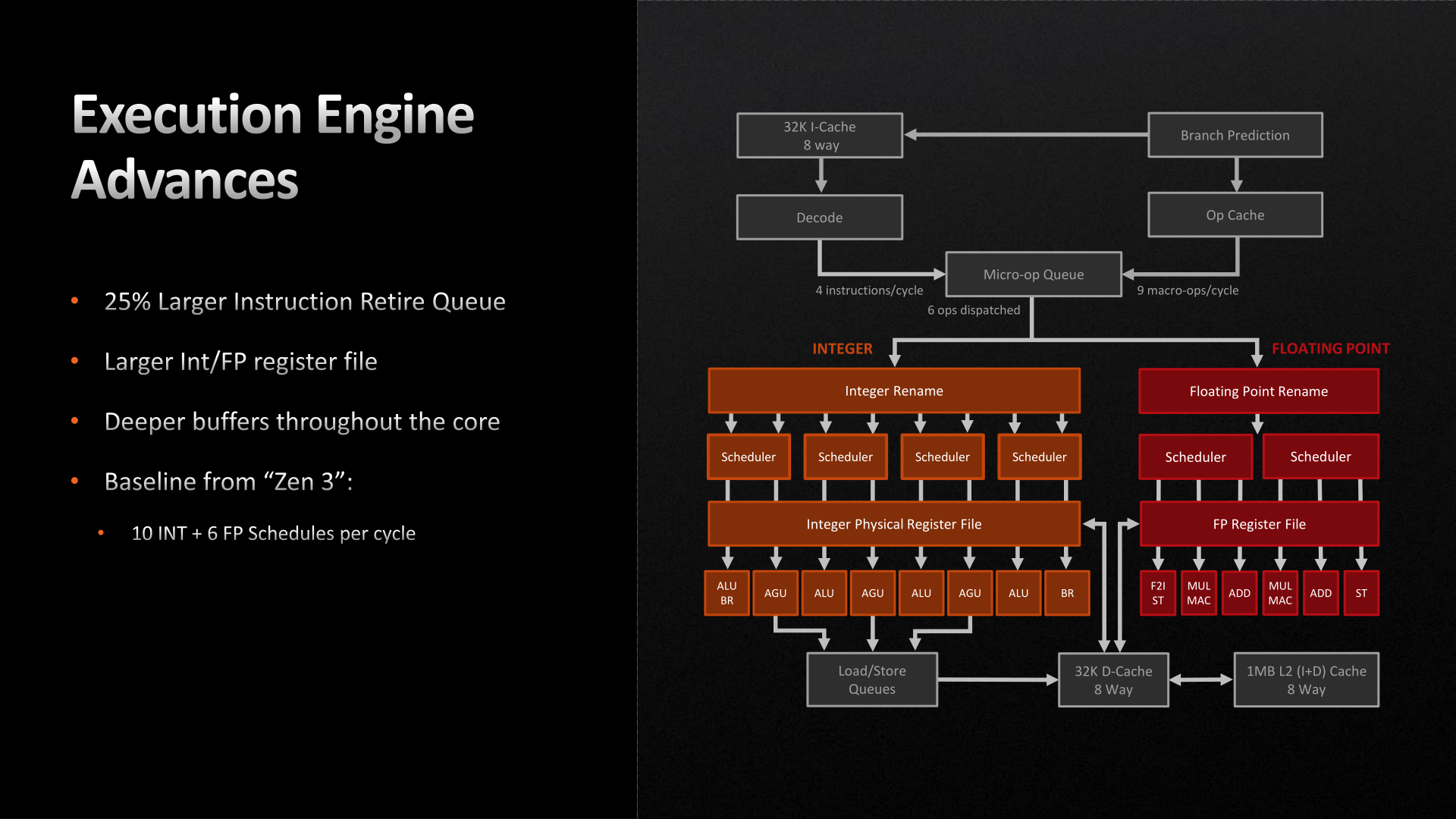
Instead, AMD’s improvements to the back-end of Zen 4 have here too focused on larger caches and buffers. Of note, the retire queue/reorder buffer is 25% larger, and is now 320 instructions deep, giving the CPU a wider window of instructions to look through to extract performance via out-of-order execution. Similarly, the Integer and FP register files have been increased in size by about 20% each, to 224 registers and 192 registers respectively, in order to accommodate the larger number of instructions that are now in flight.
The only other notable change here is AVX-512 support, which we touched upon earlier. AVX execution takes place in AMD’s floating point ports, and as such, those have been beefed up to support the new instructions.
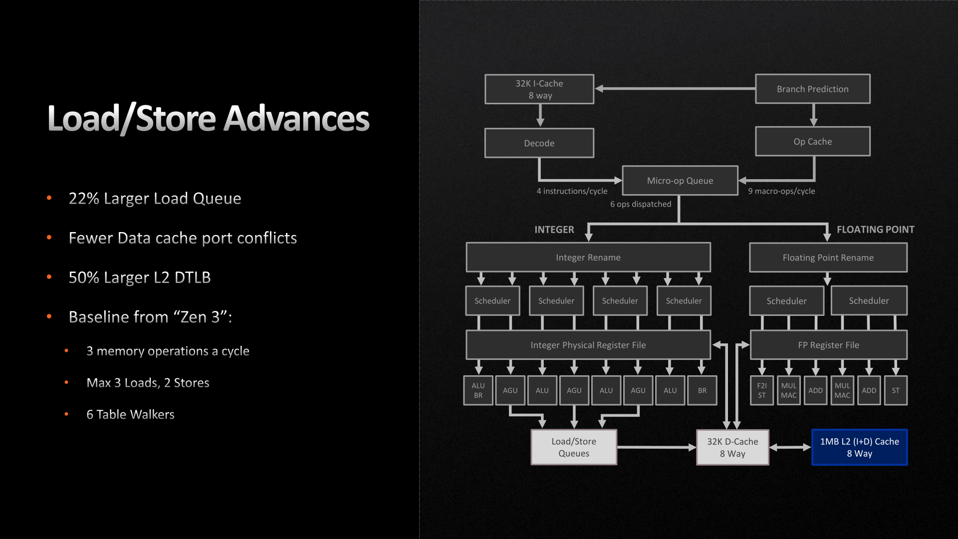
Moving on, the load/store units within each CPU core have also been given a buffer enlargement. The load queue is 22% deeper, now storing 88 loads. And according to AMD, they’ve made some unspecified changes to reduce port conflicts with their L1 data cache. Otherwise the load/store throughput remains unchanged at 3 loads and 2 stores per cycle.
Finally, let’s talk about AMD’s L2 cache. As previously disclosed by the company, the Zen 4 architecture is doubling the size of the L2 cache on each CPU core, taking it from 512KB to a full 1MB. As with AMD’s lower-level buffer improvements, the larger L2 cache is designed to further improve performance/IPC by keeping more relevant data closer to the CPU cores, as opposed to ending up in the L3 cache, or worse, main memory. Beyond that, the L3 cache remains unchanged at 32MB for an 8 core CCX, functioning as a victim cache for each CPU core’s L2 cache.
All told, we aren’t seeing very many major changes in the Zen 4 execution pipeline, and that’s okay. Increasing cache and buffer sizes is another tried and true way to improve the performance of an architecture by keeping an existing design filled and working more often, and that’s what AMD has opted to do for Zen 4. Especially coming in conjunction with the jump from TSMC 7nm to 5nm and the resulting increase in transistor budget, this is good way to put those additional transistors to good use while AMD works on a more significant overhaul to the Zen architecture for Zen 5.


205 Comments
View All Comments
Oxford Guy - Tuesday, September 27, 2022 - link
This has been posted for years. ReplyBoredInPDX - Tuesday, September 27, 2022 - link
I’m confused. I they 720p tests you write:“All gaming tests here were run using integrated graphics, with a variation of 720p resolutions and at minimum settings.”
Yet all the prior-gen AMD CPUs tested are lacking an IGP. Am I missing something? Reply
Ryan Smith - Friday, September 30, 2022 - link
You are not missing anything; we did not run any iGPU tests. That's a bit of boilerplate text that did not get scrubbed from this article. Thanks for bringing it up! ReplyGigaplex - Wednesday, September 28, 2022 - link
There's some odd results here and the article commentary doesn't seem to touch on it. Why is the 7600X absolutely trounced in Geekbench 4.0 MT? The second slowest CPU (3600XT) more than doubles it. And yet the 7950X wins by a mile in that same test, so it shouldn't be architectural. And in some of the gaming tests, the 7600X wins, and in some it comes dead last. ReplyDribble - Wednesday, September 28, 2022 - link
The processors are particularly cache bound - i.e. it fits in cache it runs very fast, if it doesn't it falls off rapidly. That is often visible in games where it'll run amazingly in some (mostly older) games, but tend to fall off, particularly in the lows, in more complex (mostly newer) games. Replyricebunny - Wednesday, September 28, 2022 - link
The SPEC multithreaded tests are N separate instantiations of the single thread tests. That’s a perfect scenario where there is no dependency or serialization in the workload and tells us very little how the CPUs would perform in a parallel workload application. There are SPEC tests specifically designed to test parallel performance, but I do not see them included in this report. Anandtech, can you comment on this? Replyabufrejoval - Wednesday, September 28, 2022 - link
Emerging dGPUs not supporting PCIe 5.0 is just crippleware!While I can easily see that 16 lanes of PCIe 5.0 won't do much for any game, I can very much see what I'd do with the 8 lanes left over when all dGPU bandwidth requirements can be met with just 8 lanes of PCIe 5.0.
Why can't they just be good PCIe citizens and negotiate to use 16 lanes of PCIe 4.0 on lesser or previous generation boards and optimize lane allocation on higher end PCIe 5.0 systems that can then use bifurcation to add say a 100Gbit NIC, plenty of Thunderbolt 4 or better yet, something CXL?
Actually I'd be really astonished if this wasn't even an artifical cap and that the Nvidia chips may actually be able to do PCIe 5.0.
It's just that they'd much rather have people use NVlink. Reply
TheinsanegamerN - Tuesday, October 4, 2022 - link
Um....dude, 4.0x16 and 5.0x8 have the same bandwidth, and no GPU today can saturate 4.0, not even close. The 300ti OCed manages to saturate.....2.0. 3.0 is a whopping 7% faster.You got awhile man. Reply
abufrejoval - Wednesday, September 28, 2022 - link
It should be interesting to see if AMD is opening the architecture for 3rd parties to exploit the actual potential of the Ryzen 7000 chips.The current mainboard/slot era that dates back to the 1981 IBM-PC (or the Apple ][) really is coming to an end and perhaps few things highlight this as well as a 600 Watt GPU that has a 65 Watt mainboard hanging under it.
We may really need something more S100 or VME, for those old enough to understand that.
Thunderbolt cables handle 4 lanes of PCIe 3.0 today and AFAIK cables are used for much higher lane counts and PCIe revisions within high-end server chassis today, even if perhaps at shorter lengths and with connectors designed for somewhat less (especially less frequent) pluggability.
Their main advantage is vastly reduced issues with mainboard traces and much better use of 3D space to optimize air flow cooling.
Sure those cables aren't cheap, but perhaps the cross-over point for additional PCB layers has been passed. And optical interconnects are waiting in the wings: they will use cables, too.
You stick PCIe 5.0 x4 fixed length cables out from all sides of an AM5 socket and connect those either to high bandwidth devices (e.g. dGPU) or a switch (PCIe 5.0 variant of the current ASMedia), you get tons of flexibility and expandability in a box form factor, that may not resemble an age old PC very much, but deliver tons of performance and expandability in a deskside form factor.
You want to recycle all your nice PCIe 3.0 2TB NVMe drives? Just add a board that puts a PCIe 5.0 20 lane switch between (even PCIe 4.0 might do fine if it's 50% $$$).
And if your dGPU actually needs 8 lanes of PCIe 5.0 to deliver top performance, connect two of those x4 cables to undo a bit of bifurcation!
How those cable connected board would then mount in a chassis and be cooled across a large range of form factors and power ranges is up for lots of great engineers to solve, while dense servers may already provide lots of the design bricks.
Unfortunately all that would require AMD to open up the base initialization code and large parts of the BIOS, which I guess currently has the ASmedia chip(s) pretty much hardwired into it.
And AMD with all their "we don't do artificial market segmentation" publicity in the past, seem to have become far more receptive to its bottom line benefits recently, to allow a free transition from console to PC/workstation and servers of all sizes.
And it would take a high-volume vendor (or AMD itself), a client side Open Compute project or similar to push that form factor the the scale where it becomes economically viable.
It's high time for a PC 2.0 (which isn't a PS/2) to bridge into the CXL universe even on desktops and workstations. Reply
Oxford Guy - Wednesday, September 28, 2022 - link
"The current mainboard/slot era that dates back to the 1981 IBM-PC (or the Apple ][)"Absolutely nothing about the IBM PC was new. The Micral N introduced slots in a microcomputer and the S-100 bus, introduced by the Altair, became the first big standard. Reply