AMD Zen 4 Ryzen 9 7950X and Ryzen 5 7600X Review: Retaking The High-End
by Ryan Smith & Gavin Bonshor on September 26, 2022 9:00 AM ESTZen 4 Architecture: Power Efficiency, Performance, & New Instructions
Now that we’ve had a chance to take a look at the AM5 platform surrounding the new Ryzen 7000 chips, as well as the new IOD that completes the high-end Ryzen chips, let’s dive into the heart of matters: the Zen 4 CPU cores.
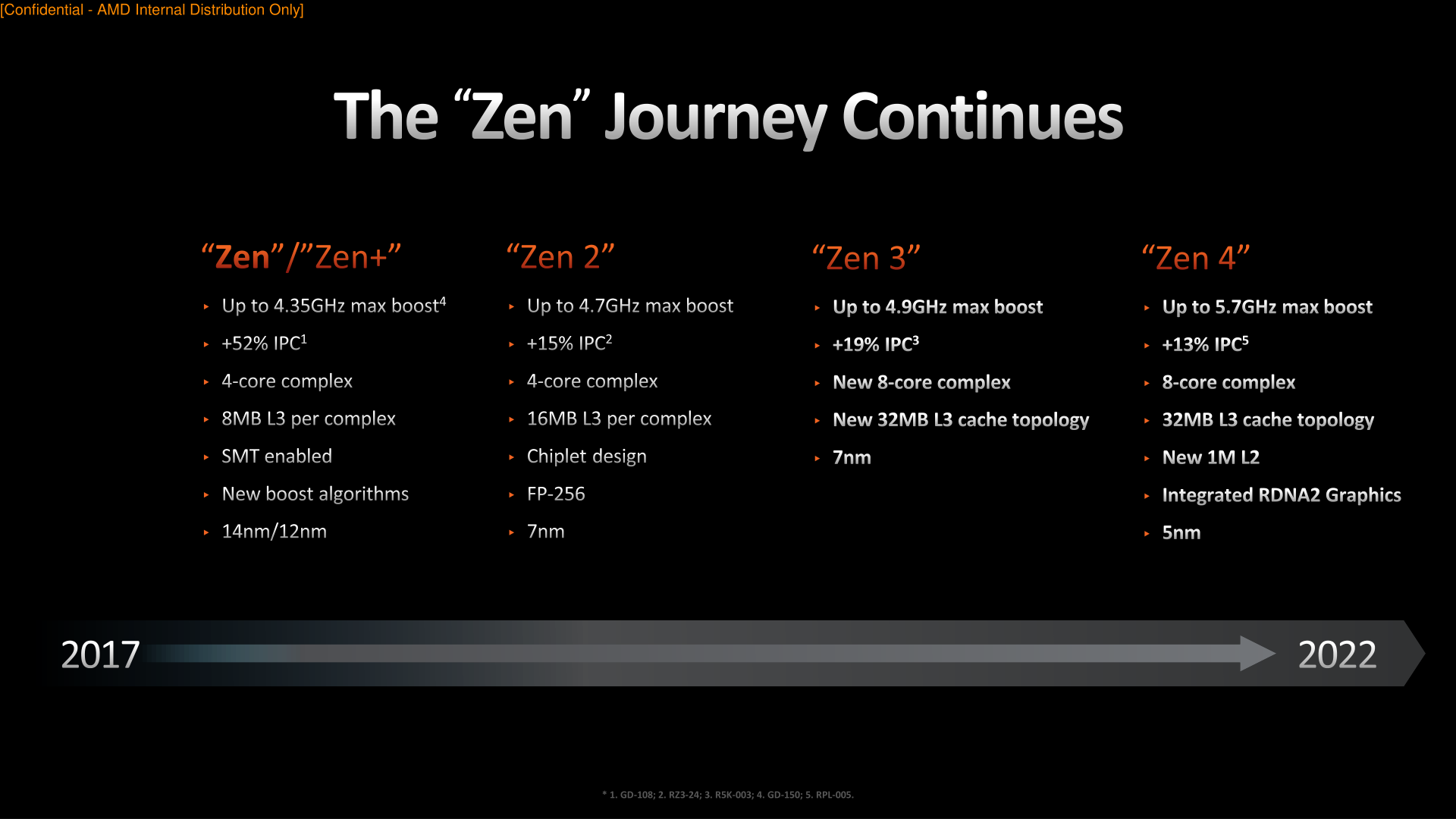
As laid out in previous pages, a big element in AMD’s design goals for the Ryzen 7000 platform was to modernize it, adding support for things like PCIe 5.0 and DDR5, as well as integrating more fine-grained power controls. And while this attention meant that AMD’s collective attention was split between the CPU cores and the rest of the platform, AMD’s CPU cores are far from being ignored here. Still, it’s fair to say that AMD’s goal for the Zen 4 architecture has not been a radical overhaul of their core CPU architecture. For that, you’ll want to wait for Zen 5 in 2024.
Instead, Zen 4 is a further refinement of AMD’s Zen 3 architecture, with AMD taking advantage of things like the new AM5 platform and TSMC’s 5nm process to further boost performance. There are some important changes here that are allowing AMD to deliver an average IPC increase of 13%, and combined with improvements to enable higher clockspeeds and greater power efficiency for both single-threaded and multi-threaded workloads, no part of AMD’s CPU performance has gone untouched.
Zen 4 Power: More Efficient, More Power-Hungry
We’ll start with a look at power efficiency, since power consumption plays a huge part in the Zen 4 story at both ends of the curve.
By tapping TSMC’s current-generation 5nm, process, AMD is enjoying the advantage of a full node shrink for their CPU cores. Thus far TSMC 5nm (and its 4nm derivative) is proving to be the powerhouse process of its generation, as TSMC’s clients have seen some solid gains in power efficiency and transistor density moving from 7nm to 5nm. Meanwhile TSMC’s competitors are either struggling by delivering less efficient 4nm-class nodes (Samsung), or they’ve yet to deliver a 4nm-class node at all (Intel). In other words, for the moment TSMC’s 5nm-class nodes are as good as it gets, putting AMD in a great position to take advantage of the benefits.
Coupled with this are all of the various platform power improvements that come with AM5 and the new 6nm IOD. These include the 3 variable power rails, SVI3 VRM monitoring, and AMD’s lower-power Infinity Fabric Links. As a result, the Ryzen 7000 chips enjoy a significant power efficiency advantage versus the Ryzen 5000 chips.
How much of an improvement, in turn, depends on where on the voltage/frequency curve you end up. As we alluded to earlier when talking about AM5, one of AMD’s design goals was to provide more power to Ryzen 7000 chips so that they could go farther into the vf curve and keep their cores running at a higher frequency in MT-heavy workloads.
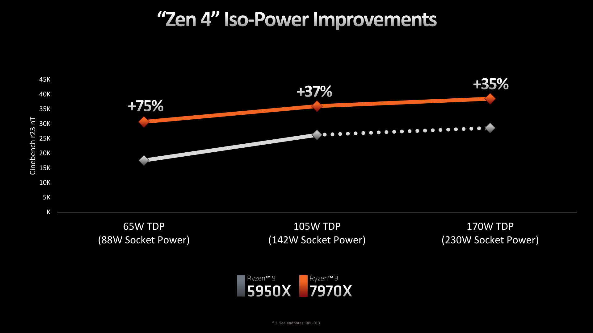
The net result is that, according to AMD’s data, the company is seeing extensive power efficiency gains at lower TDPs. In this case, pitting a 5950X against a 7950X with a maximum socket power of 88 Watts, AMD is seeing a 75% increase in performance on Cinebench R23 nT. This is something of a worst-case scenario for the older Ryzen chip, as it tended to be TDP limited even at is native TDP, and the relatively high idle power draw of the IOD and the rest of the platform further ate into that. As a result, the 5950X needs to pull back on clockspeeds significantly at lower TDPs. For Ryzen 7000/Zen 4 on the other hand, AMD’s newer architecture fairs much better; it still takes a hit from the TDP drop, but not by nearly as much.
Meanwhile, increasing the socket power to 142 (5950X’s stock power) and then to 230W (7950X’s stock power) still produces a significant speed up in performance, but we’re certainly into the area of diminishing returns. In this case the 7950X has a 37% lead and 35% lead at 142W and 230W respectively.
We’ll take a look at more power data for the new Ryzen 7000 chips a bit later in our review, but the basic pattern is clear: Zen 4 can be a very power efficient architecture. But AMD is also discarding some of that efficiency advantage in the name of improving raw performance. Especially in multi-threaded workloads, for high-end chips like the 7950X the performance gains we’re seeing are as much from higher TDPs as they are higher IPCs and improved power efficiency.
This will make AMD’s eventual Zen 4 mobile products (Phoenix Point) an especially interesting product to keep an eye on. The greater focus on power efficiency (and harder cap on top TDPs) means that we may not yet have seen Zen 4 put its best foot forward when it comes to power efficiency.
Clockspeeds: Going Faster Means Being Faster
One way that’s always a good method to improve your CPU performance is just to flat-out increase clockspeeds. Tried and true, this drove the x86 CPU industry for most of its first 30 years before the laws of physics (and specifically, the death of Dennard Scaling) put the brakes on massive generation-on-generation clockspeed gains. Still, AMD and Intel like to squeeze out higher frequencies when they can, and in the case of AMD’s CPU architecture, TSMC’s 5nm process has provided for some nice gains here, finally pushing AMD well over the (stubborn) 5GHz mark.
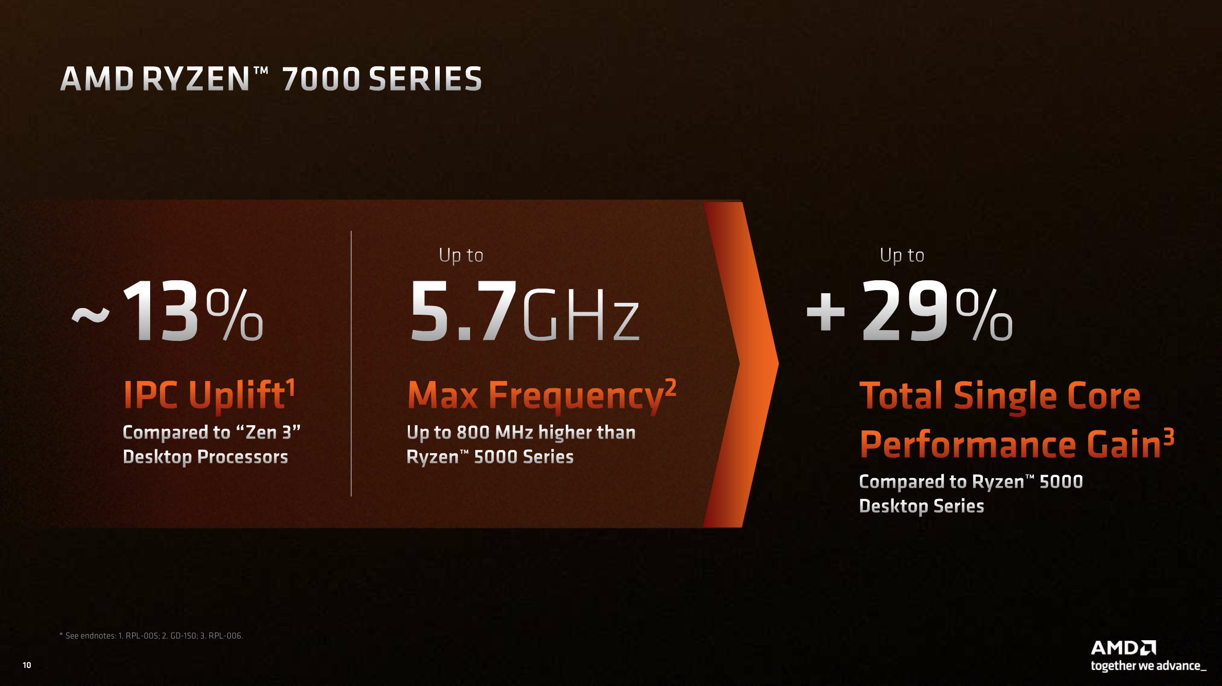
For AMD’s high-end Ryzen 7000 desktop processors, the top turbo frequencies are now as high as 5.7GHz for the Ryzen 9 7950X, and even the slowest Ryzen 5 7600X is rated to hit 5.3GHz. And in both cases, there is still a bit more headroom still when using Precision Boost Optimization 2 (PBO2), allowing chips to potentially eek out another 100MHz or so. For AMD’s top-end part then, we’re looking at a 16% increase in turbo clockspeeds, while the 7600X is clocked some 15% faster than its predecessor.
According to AMD’s engineers, there is no singular magic trick here that has allowed them to boost clockspeeds to the high 5GHz range on Zen 4, nor has the company sacrificed any IPC to allow for higher clockspeeds (e.g. lengthening pipelines). TSMC’s 5nm process sure helped a lot in this regard, but AMD’s technical relationship with TSMC also improved as the company’s CPU engineers became familiar with designing and optimizing CPUs for TSMC’s 7nm and 6nm process nodes. As a result, the two companies were able to better work together to reliably get higher frequencies out of AMD’s CPU cores, with AMD going as far as to integrating some TSMC IP instead of relying on more traditional design partners.
Even with that, Zen 4 actually came in a bit below AMD’s expectations, if you can believe that. According to the company’s engineers, they were hoping to hit 6GHz on this part, something that didn’t quite come to fruition. So AMD’s users will have to settle for just 5.7GHz, instead.
Zen 4 IPC: Getting 13% More
On the other side of the performance equation we have IPC improvements. AMD’s broader focus on platform design for the Ryzen 7000 generation means that the IPC gains aren’t quite as great as what we saw on Zen 3 or Zen 2, but they’re not to be ignored, either. Even without a massive overhaul of AMD’s execution back-end – and with only a moderate update to the front-end – AMD was still able to squeeze out an average IPC gain of 13% across a couple of dozen benchmarks, only 2 percentage points lower than the 15% gains AMD delivered with the Zen 2 architecture in 2019.
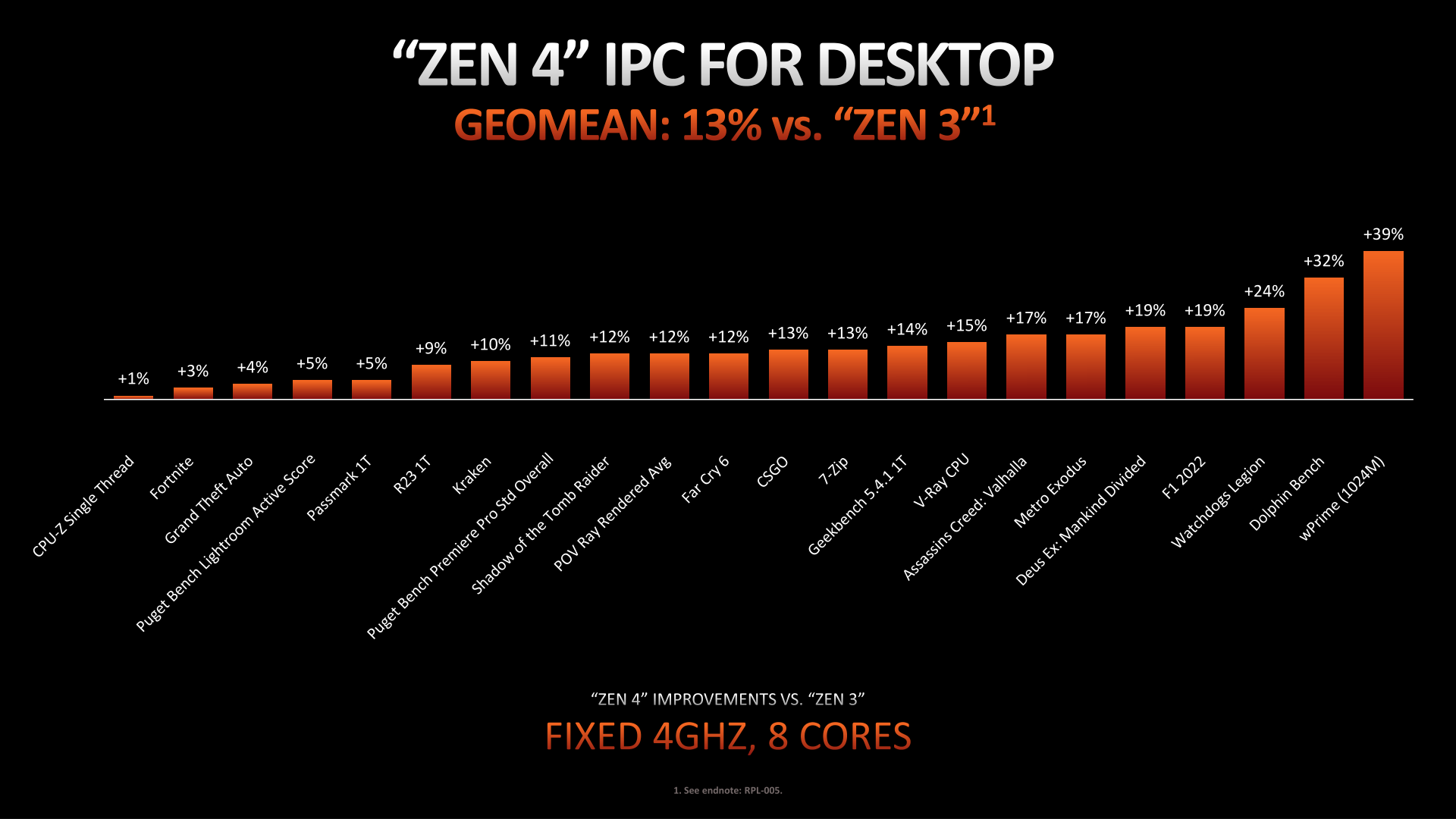
We won’t fixate on any one workload here, but it does run the gamut. At an iso-frequency of 4GHz, Zen 4 delivers anything from a tiny increase to 39% at the top end. In traditional PC performance fashion, the gains from one generation to the next are workload-dependent. So a 13% average does leave plenty of wiggle-room for either greater or lesser gains, as we’ll see in our full benchmark results.
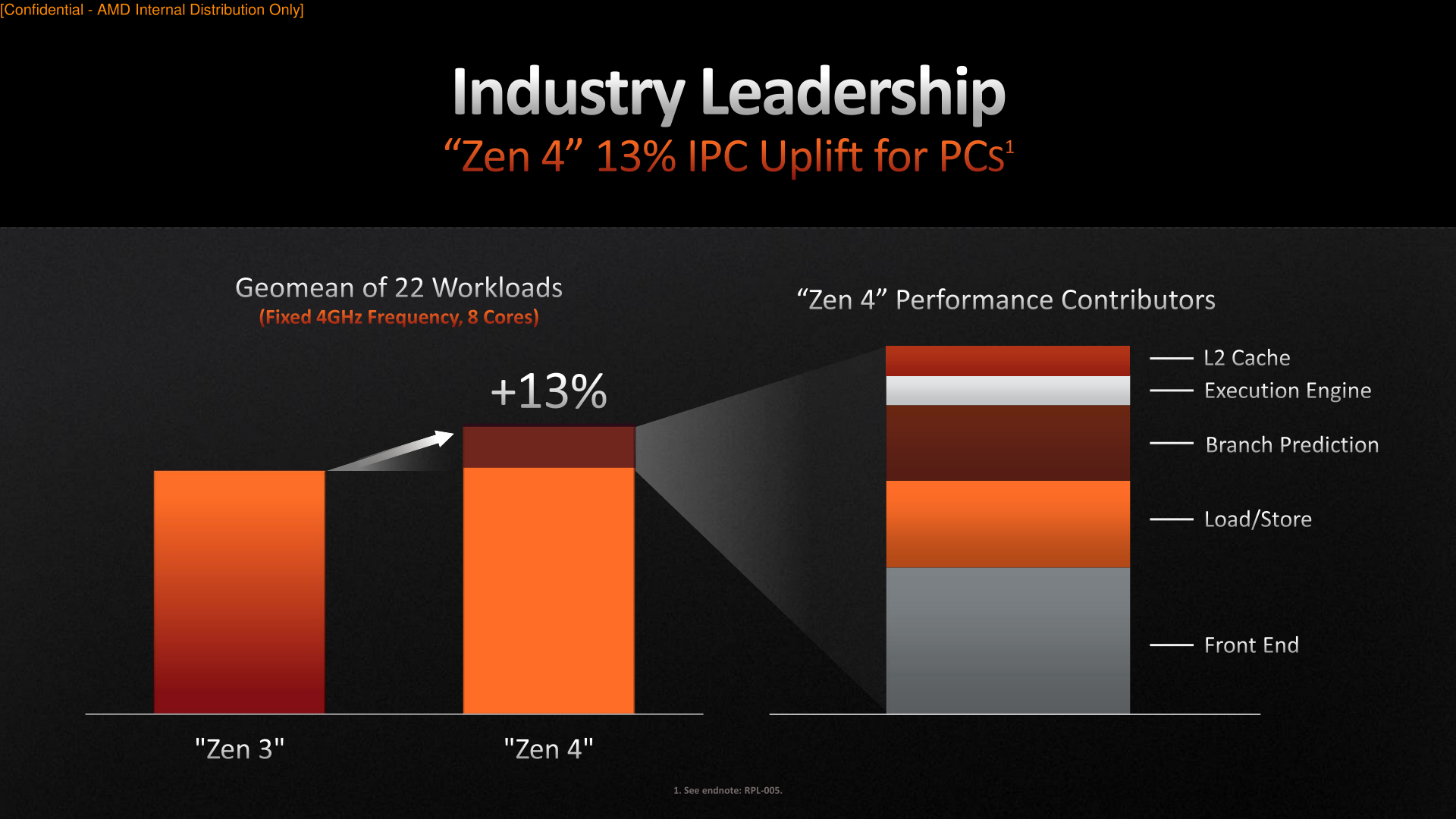
AMD has also provided a handy IPC contributor breakdown, showing where those 13% average gains come from. The single biggest contributor here was Zen 4’s front-end changes, followed by load/store improvements, and then branch prediction improvements.
New Instructions: AVX-512, Automatic IBRS
Although Zen 4 is a more modest update to AMD’s CPU architecture, the company still managed to work in a fairly significant update to their instruction set support, with the addition of AVX-512 support.
The latest iteration of the Intel-developed Advanced Vector Extensions (AVX), AVX-512 is a fairly major addition to the AVX suite. Besides increasing the native vector width to 512-bits, AVX also improves the AVX instruction set with a number of new features and data types – a collection of features that keeps growing as Intel continues to add further extensions to AVX-512 itself.
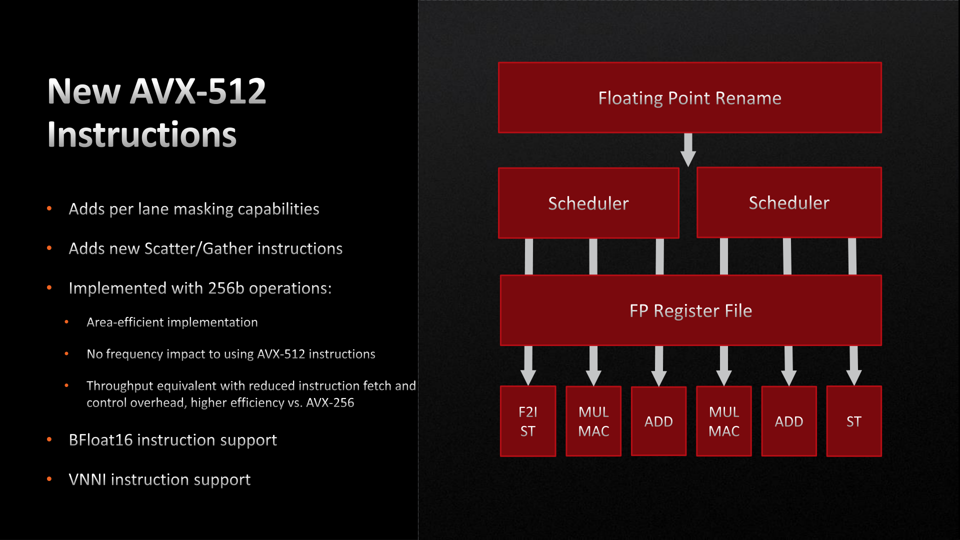
Of particular interest for client CPUs and workloads, AVX-512 adds per-lane masking capabilities – allowing for individual lanes to be masked off rather than breaking up a vector for multiple passes – as well as new data manipulation instructions. This includes additional scatter/gather instructions, and instructions that are useful for neural network processing, such as bfloat16 support and a whole instruction sub-set (VNNI) for deep learning.
AVX-512 has an interesting history that, while we won’t cover in complete details, has left a patchwork of support across the client CPU landscape. While Intel added support in its client CPUs starting with Ice Lake and Rocket Lake (11th Gen Core), Intel also removed support for AVX-512 from their client CPUs starting with Alder Lake (13th Gen Core), owing to the fact that Alder Lake’s mixed-core strategy required that the only instructions used were supported by both the P-cores and E-cores. Which, in the case of the Atom-based Gracemont E-cores, was not available, leading to Intel disabling AVX-512 on Alder Lake parts even though the P-cores did support the new instructions.
As a result, the introduction of AVX-512 support actually gives AMD an edge over Intel right now. While AMD’s new CPUs can use the newer instruction set, Intel’s cannot, with Alder Lake limited to AVX2 and below.
But the situation is not a slam-dunk for AMD, either. In order to avoid the significant die space and power costs of actually implementing and operating a 512-bit wide SIMD, AMD has made the interesting decision to implement AVX-512 on top of a 256-bit SIMD, which happens to be the same width as Zen 3’s AVX2 SIMD. This means that while AMD can execute AVX-512 instructions, they have to do so over 2 cycles of their 256-bit SIMD. Which means that, on paper, AMD’s vector throughput per cycle per core has not improved from one generation to the next.
None the less, it’s a situation that benefits AMD for a couple of reasons. The first is the performance unlocked by the AVX-512 instructions. AVX-512 instructions are denser (there’s less fetching and control overhead), and some of these additions are instructions that manipulate data in ways that would take several cycles (or more) if implemented using AVX2 instructions. So AMD is still getting performance gains by supporting AVX-512, even without the doubled vector width.
The second benefit is that by keeping their SIMD narrower, AMD isn’t lighting up a billion dense, power-hungry transistors all at once. This is an ongoing challenge for 512-bit native SIMD designs that in Intel’s chips required them to back off on their clockspeeds to stay within their power budgets. So while a wider SIMD would technically be more efficient on pure AVX-512 throughput, the narrower SIMD allows AMD to keep their clockspeeds higher, something that’s particularly useful in mixed workloads where the bottleneck shifts between vector throughput and more traditional serial instructions.
Ultimately, for client CPUs, this is a nice feature to have, but it admittedly wasn’t a huge, market-shifting feature advantage with Rocket Lake. And it’s unlikely to be that way for AMD, either. Instead, the biggest utility for AVX-512 is going to be in the server space, where AMD’s Genoa processors will be going up against Intel Ice Lake (and eventually, Sapphire Rapids) parts with full AVX-512 implementations.
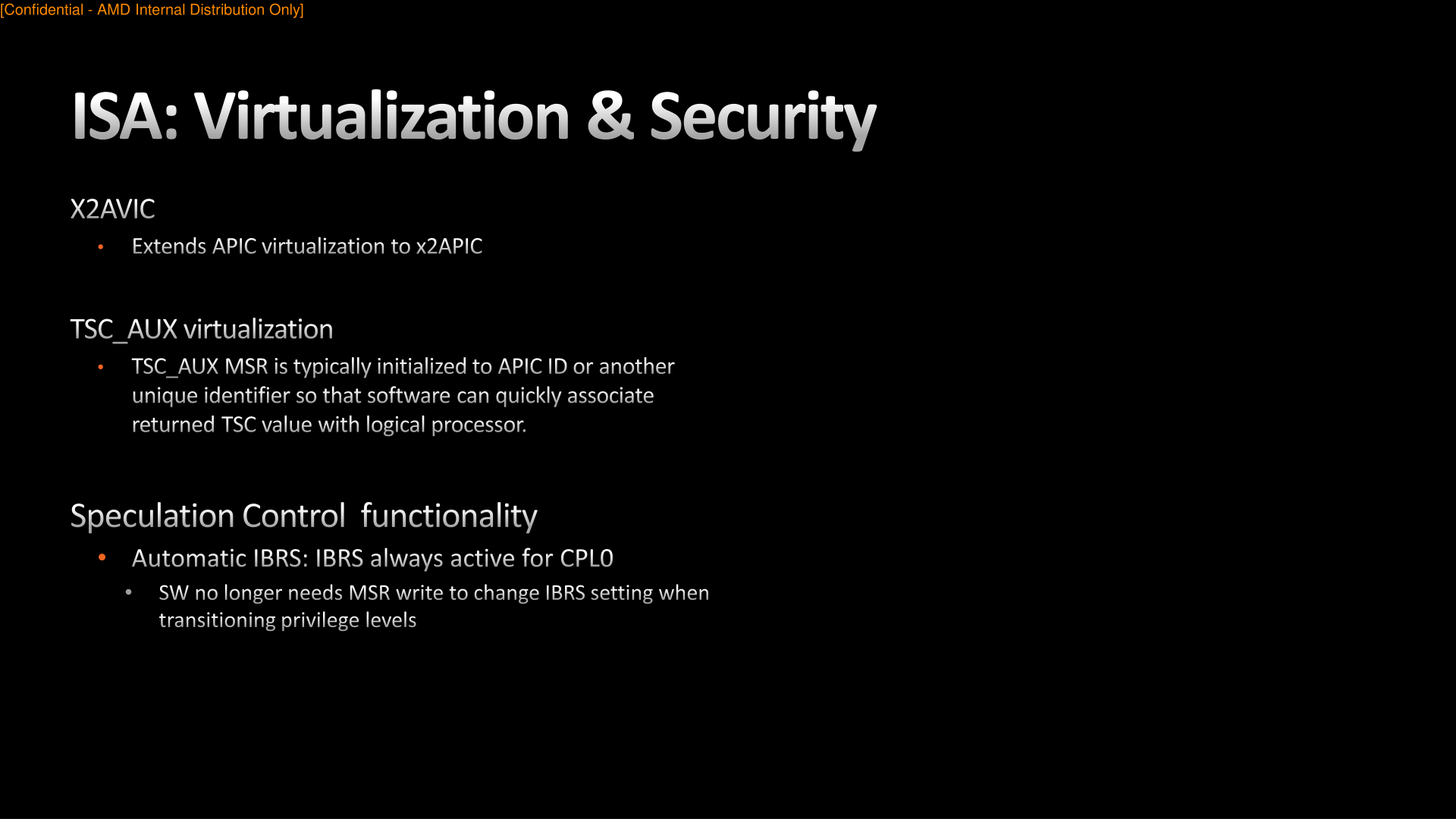
Finally, AMD is also adding/changing a handful of instructions related to security and virtualization. I won’t parrot AMD’s own slide on the matter, but for general desktop users, the most notable of these changes is how AMD is handling speculation control to prevent side-channel attacks. The Indirect Branch Restricted Speculation (IBRS) instruction, which is used on critical code paths to restrict the speculation of indirect branches, is now automatic. Any time a CPU core goes to CPL0/Ring 0 – the kernel ring and thus the most privileged ring – IBRS is automatically turned on, and similarly turned off when the CPU core exits CPL0.
Previously, software would need to specifically invoke IRBS using a model specific register, which although not a deal-breaker, was one more thing for an application (and application programmers) to keep track of in an already complex security landscape. Thus this change doesn’t directly add any new security features, but it makes it much easier to take advantage of an existing one.


205 Comments
View All Comments
Oxford Guy - Tuesday, September 27, 2022 - link
This has been posted for years. ReplyBoredInPDX - Tuesday, September 27, 2022 - link
I’m confused. I they 720p tests you write:“All gaming tests here were run using integrated graphics, with a variation of 720p resolutions and at minimum settings.”
Yet all the prior-gen AMD CPUs tested are lacking an IGP. Am I missing something? Reply
Ryan Smith - Friday, September 30, 2022 - link
You are not missing anything; we did not run any iGPU tests. That's a bit of boilerplate text that did not get scrubbed from this article. Thanks for bringing it up! ReplyGigaplex - Wednesday, September 28, 2022 - link
There's some odd results here and the article commentary doesn't seem to touch on it. Why is the 7600X absolutely trounced in Geekbench 4.0 MT? The second slowest CPU (3600XT) more than doubles it. And yet the 7950X wins by a mile in that same test, so it shouldn't be architectural. And in some of the gaming tests, the 7600X wins, and in some it comes dead last. ReplyDribble - Wednesday, September 28, 2022 - link
The processors are particularly cache bound - i.e. it fits in cache it runs very fast, if it doesn't it falls off rapidly. That is often visible in games where it'll run amazingly in some (mostly older) games, but tend to fall off, particularly in the lows, in more complex (mostly newer) games. Replyricebunny - Wednesday, September 28, 2022 - link
The SPEC multithreaded tests are N separate instantiations of the single thread tests. That’s a perfect scenario where there is no dependency or serialization in the workload and tells us very little how the CPUs would perform in a parallel workload application. There are SPEC tests specifically designed to test parallel performance, but I do not see them included in this report. Anandtech, can you comment on this? Replyabufrejoval - Wednesday, September 28, 2022 - link
Emerging dGPUs not supporting PCIe 5.0 is just crippleware!While I can easily see that 16 lanes of PCIe 5.0 won't do much for any game, I can very much see what I'd do with the 8 lanes left over when all dGPU bandwidth requirements can be met with just 8 lanes of PCIe 5.0.
Why can't they just be good PCIe citizens and negotiate to use 16 lanes of PCIe 4.0 on lesser or previous generation boards and optimize lane allocation on higher end PCIe 5.0 systems that can then use bifurcation to add say a 100Gbit NIC, plenty of Thunderbolt 4 or better yet, something CXL?
Actually I'd be really astonished if this wasn't even an artifical cap and that the Nvidia chips may actually be able to do PCIe 5.0.
It's just that they'd much rather have people use NVlink. Reply
TheinsanegamerN - Tuesday, October 4, 2022 - link
Um....dude, 4.0x16 and 5.0x8 have the same bandwidth, and no GPU today can saturate 4.0, not even close. The 300ti OCed manages to saturate.....2.0. 3.0 is a whopping 7% faster.You got awhile man. Reply
abufrejoval - Wednesday, September 28, 2022 - link
It should be interesting to see if AMD is opening the architecture for 3rd parties to exploit the actual potential of the Ryzen 7000 chips.The current mainboard/slot era that dates back to the 1981 IBM-PC (or the Apple ][) really is coming to an end and perhaps few things highlight this as well as a 600 Watt GPU that has a 65 Watt mainboard hanging under it.
We may really need something more S100 or VME, for those old enough to understand that.
Thunderbolt cables handle 4 lanes of PCIe 3.0 today and AFAIK cables are used for much higher lane counts and PCIe revisions within high-end server chassis today, even if perhaps at shorter lengths and with connectors designed for somewhat less (especially less frequent) pluggability.
Their main advantage is vastly reduced issues with mainboard traces and much better use of 3D space to optimize air flow cooling.
Sure those cables aren't cheap, but perhaps the cross-over point for additional PCB layers has been passed. And optical interconnects are waiting in the wings: they will use cables, too.
You stick PCIe 5.0 x4 fixed length cables out from all sides of an AM5 socket and connect those either to high bandwidth devices (e.g. dGPU) or a switch (PCIe 5.0 variant of the current ASMedia), you get tons of flexibility and expandability in a box form factor, that may not resemble an age old PC very much, but deliver tons of performance and expandability in a deskside form factor.
You want to recycle all your nice PCIe 3.0 2TB NVMe drives? Just add a board that puts a PCIe 5.0 20 lane switch between (even PCIe 4.0 might do fine if it's 50% $$$).
And if your dGPU actually needs 8 lanes of PCIe 5.0 to deliver top performance, connect two of those x4 cables to undo a bit of bifurcation!
How those cable connected board would then mount in a chassis and be cooled across a large range of form factors and power ranges is up for lots of great engineers to solve, while dense servers may already provide lots of the design bricks.
Unfortunately all that would require AMD to open up the base initialization code and large parts of the BIOS, which I guess currently has the ASmedia chip(s) pretty much hardwired into it.
And AMD with all their "we don't do artificial market segmentation" publicity in the past, seem to have become far more receptive to its bottom line benefits recently, to allow a free transition from console to PC/workstation and servers of all sizes.
And it would take a high-volume vendor (or AMD itself), a client side Open Compute project or similar to push that form factor the the scale where it becomes economically viable.
It's high time for a PC 2.0 (which isn't a PS/2) to bridge into the CXL universe even on desktops and workstations. Reply
Oxford Guy - Wednesday, September 28, 2022 - link
"The current mainboard/slot era that dates back to the 1981 IBM-PC (or the Apple ][)"Absolutely nothing about the IBM PC was new. The Micral N introduced slots in a microcomputer and the S-100 bus, introduced by the Altair, became the first big standard. Reply