The Intel 12th Gen Core i9-12900K Review: Hybrid Performance Brings Hybrid Complexity
by Dr. Ian Cutress & Andrei Frumusanu on November 4, 2021 9:00 AM ESTCPU Tests: SPEC ST Performance on P-Cores & E-Cores
SPEC2017 is a series of standardized tests used to probe the overall performance between different systems, different architectures, different microarchitectures, and setups. The code has to be compiled, and then the results can be submitted to an online database for comparison. It covers a range of integer and floating point workloads, and can be very optimized for each CPU, so it is important to check how the benchmarks are being compiled and run.
For compilers, we use LLVM both for C/C++ and Fortan tests, and for Fortran we’re using the Flang compiler. The rationale of using LLVM over GCC is better cross-platform comparisons to platforms that have only have LLVM support and future articles where we’ll investigate this aspect more. We’re not considering closed-sourced compilers such as MSVC or ICC.
clang version 10.0.0
clang version 7.0.1 (ssh://git@github.com/flang-compiler/flang-driver.git
24bd54da5c41af04838bbe7b68f830840d47fc03)
-Ofast -fomit-frame-pointer
-march=x86-64
-mtune=core-avx2
-mfma -mavx -mavx2
Our compiler flags are straightforward, with basic –Ofast and relevant ISA switches to allow for AVX2 instructions. We decided to build our SPEC binaries on AVX2, which puts a limit on Haswell as how old we can go before the testing will fall over. This also means we don’t have AVX512 binaries, primarily because in order to get the best performance, the AVX-512 intrinsic should be packed by a proper expert, as with our AVX-512 benchmark. All of the major vendors, AMD, Intel, and Arm, all support the way in which we are testing SPEC.
To note, the requirements for the SPEC licence state that any benchmark results from SPEC have to be labeled ‘estimated’ until they are verified on the SPEC website as a meaningful representation of the expected performance. This is most often done by the big companies and OEMs to showcase performance to customers, however is quite over the top for what we do as reviewers.
For Alder Lake, we start off with a comparison of the Golden Cove cores, both in DDR5 as well as DDR4 variants. We’re pitting them as direct comparison against Rocket Lake’s Cypress Cove cores, as well as AMD’s Zen3.
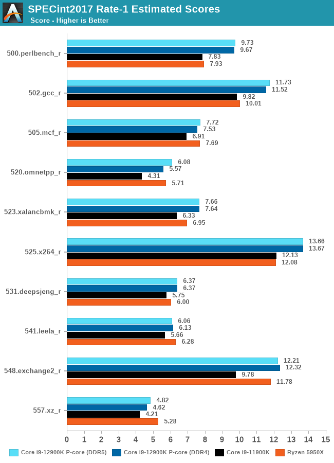
Starting off in SPECint2017, the first thing I’d say is that for single-thread workloads, it seems that DDR5 doesn’t showcase any major improvements over DDR4. The biggest increase for the Golden Cove cores are in 520.omnetpp_r at 9.2% - the workload is defined by sparse memory accessing in a parallel way, so DDR5’s doubled up channel count here is likely what’s affecting the test the most.
Comparing the DDR5 results against RKL’s WLC cores, ADL’s GLC showcases some large advantages in several workloads: 24% in perlbench, +29% in omnetpp, +21% in xalancbmk, and +26% in exchange2 – all of the workloads here are likely boosted by the new core’s larger out of order window which has grown to up to 512 instructions. Perlbench is more heavily instruction pressure biased, at least compared to other workloads in the suite, so the new 6-wide decoder also likely is a big reason we see such a large increase.
The smallest increases are in mcf, which is more pure memory latency bound, and deepsjeng and leela, the latter which is particularly branch mispredict heavy. Whilst Golden Cove improves its branch predictors, the core also had to add an additional cycle of misprediction penalty, so the relative smaller increases here make sense with that as a context.
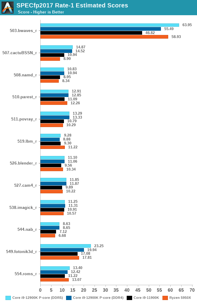
In the FP suite, the DDR5 results have a few larger outliers compared to the DDR4 set, bwaves and fotonik3d showcase +15% and +17% just due to the memory change, which is no surprise given both workloads extremely heavy memory bandwidth characteristic.
Compared to RKL, ADL showcases also some very large gains in some of the workloads, +33% in cactuBBSN, +24% in povray. The latter is a surprise to me as it should be a more execution-bound workload, so maybe the new added FADD units of the cores are coming into play here.
We’ve had not too much time to test out the Gracemont cores in isolation, but we are able to showcase some results. This set here is done on native Linux rather than WSL due to affinity issues on Windows, the results are within margin of error between the platforms, however there are a few % points outliers on the FP suite. Still, comparing the P to E-cores are in apples-to-apples conditions in these set of graphs:
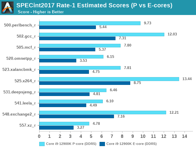
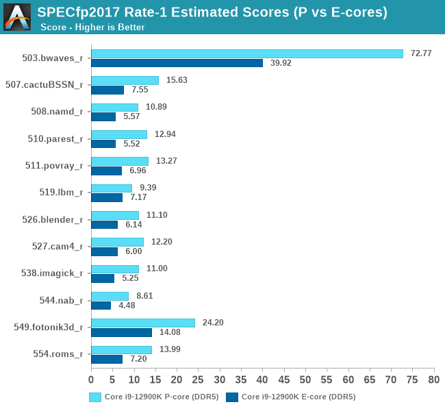
When Intel mentioned that the Gracemont E-cores of Alder Lake were matching the ST performance of the original Skylake, Intel was very much correct in that description. Unlike what we consider “little” cores in a normal big.LITTLE setup, the E-cores of Alder Lake are still quite performant.
In the aggregate scores, an E-core is roughly 54-64% of a P-core, however this percentage can go as high as 65-73%. Given the die size differences between the two microarchitectures, and the fact that in multi-threaded scenarios the P-cores would normally have to clock down anyway because of power limits, it’s pretty evident how Intel’s setup with efficiency and density cores allows for much higher performance within a given die size and power envelope.
In SPEC, in terms of package power, the P-cores averaged 25.3W in the integer suite and 29.2W in the FP suite, in contrast to respectively 10.7W and 11.5W for the E-cores, both under single-threaded scenarios. Idle package power ran in at 1.9W.
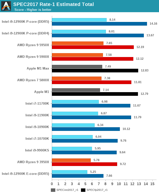
Alder Lake and the Golden Cove cores are able to reclaim the single-threaded performance crown from AMD and Apple. The increases over Rocket Lake come in at +18-20%, and Intel’s advantage over AMD is now at 6.4% and 16.1% depending on the suite, maybe closer than what Intel would have liked given V-cache variants of Zen3 are just a few months away.
Again, the E-core performance of ADL is impressive, while not extraordinary ahead in the FP suite, they can match the performance of some middle-stack Zen2 CPUs from only a couple of years ago in the integer suite.


474 Comments
View All Comments
mode_13h - Sunday, November 7, 2021 - link
I'm not even going to say this is a bad idea. The problem is that it's a big change and Intel normally prepares the software developer community for big new ISA extensions a year+ in advance!Again, what you're talking about is an ABI change, which is a big deal. Not only that, but to require code to handle dynamically switching between AVX2 and AVX-512 paths means that it can't use different datastructures for each codepath. It even breaks the task pre-emption model, since there need to be some limitations on where the code needs to have all its 512-bit registers flushed so it can handle switching to the AVX2 codepath (or vice versa).
This adds a lot of complexity to the software, and places a greater testing burden on software developers. All for (so far) one CPU. It just seems a bit much, and I'm sure a lot of software companies would just decide not to touch AVX-512 until things settle down.
GeoffreyA - Sunday, November 7, 2021 - link
My view on this topic is that Intel made a sound decision disabling AVX512. Some of the comments are framing it as if they made a mistake, because the tech community discovered it was still there, but I don't see any problem. Only, the wording was at fault, this controversial "fused off" statement. And actually, the board makers are at fault, too, enabling a hidden feature and causing more confusion.On the question of whether it's desirable, allowing one core with the instructions and another without, would've been a recipe for disaster---and that, too, for heaven knows what gain. The simplest approach was bringing both cores onto the same footing. Indeed, I think this whole P/E paradigm is worthless, adding complexity for minimal gain.
Oxford Guy - Monday, November 8, 2021 - link
‘Intel made a sound decision disabling AVX512’That’s not what happened.
O-o-o-O - Sunday, November 7, 2021 - link
Really? Our tech guys tried out Xeon Phi but couldn't make use of it. Years later, Xeon Phi was abruptly discontinued due to lack of demand. GPGPUs are much easier to handle.Yeah, coding cost and risks aside, it's interesting to see complex work of art in the modern CPU. But I'd rather wish for expansion of GPU support (like shared memory and higher band-width).
kwohlt - Sunday, November 7, 2021 - link
My understanding is that Raptor Lake's change is replacing Golden Cover P cores with Raptor Cove P cores, doubling Gracemont E-Cores per SKU, and using the same Intel 7 process. Granted, it's all leaks at this point, but with Gracemont being reused for Raptor Lake, I don't expect AVX-512 next year either.mode_13h - Monday, November 8, 2021 - link
> Raptor Lake's change is ... doubling Gracemont E-Cores ... using the same Intel 7 process.I was merely speculating that this *might* just be a transient problem. If they're using the same process node for Raptor Lake, which seems very plausible, then it's understandable if they don't want to increase the size or complexity of their E-cores.
However, there's some precedent, in the form of Knights Landing, where Intel bolted on dual AVX-512 pipelines + SMT4 to a Silvermont Atom core. And with a more mature Intel 7 node, perhaps the yield will support the additional area needed for just a single pipe + 512-bit registers. And let's not forget how Intel increased the width of Goldmont, yet simply referred to it as Goldmont+.
So, maybe Raptor Lake will use Gracemont+ cores that are augmented with AVX-512. We can hope.
GURU7OF9 - Saturday, November 6, 2021 - link
The is by far the best review I have read so far.A great comparison I would love to see just out of curiouslty would be to see P core only benchmarks and then e core only benchmarks! We could gain a much better understanding of the capabilities and performance of both .
This would bring a little bit of familiarity back to benchmarking .
nunya112 - Saturday, November 6, 2021 - link
the only info provided was its on intels new process 7 node. what does that mean? are they using TSMC and at 7nm? or did they finally crack 7nm at Intel?mode_13h - Sunday, November 7, 2021 - link
"Intel 7" is the process node formerly known as "10 nm ESF" (Enhanced SuperFin), which is the 4th generation 10 nm process, counting by the revisions they've introduced between the different products based on it. They like to pretend that Cannon Lake didn't happen, but that's why Ice Lake was actually 10 nm+ (2nd gen).They rebranded 10 nm ESF as "Intel 7" for marketing reasons, as explained here:
https://www.anandtech.com/show/16823/intel-acceler...
Hossein - Sunday, November 7, 2021 - link
It's funny that most reviewers are conveniently silent about the fact that there are quite a 'few' games which are incompatible AL.