Google's Tensor inside of Pixel 6, Pixel 6 Pro: A Look into Performance & Efficiency
by Andrei Frumusanu on November 2, 2021 8:00 AM EST- Posted in
- Mobile
- Smartphones
- SoCs
- Pixel 6
- Pixel 6 Pro
- Google Tensor
GPU Performance & Power
The Google Tensors GPU is quite a beast. A Mali G78 with 20 cores, it’s sporting 42% more cores than the Exynos 2100 implementation, and only comes second after HiSilicon’s Kirin 9000. However, unlike the more power efficient N5 process node of the Kirin 9000, the Tensor SoC comes on the same process node as on the Exynos 2100. Having a much larger GPU, one would expect Google to drive the block at lower frequencies, in order to achieve better energy efficiency. To our surprise, the G78MP20 runs at up to 1GHz on the tiler and L2, and up to 848MHz on the shader cores, which is essentially the same as the smaller Exynos 2100 implementation of the GPU. Of course this immediately raises red flags for the Tensor when it comes to power consumption, as the chip certainly can’t pull out a rabbit out of a hat in terms of efficiency, so let’s see what happens:
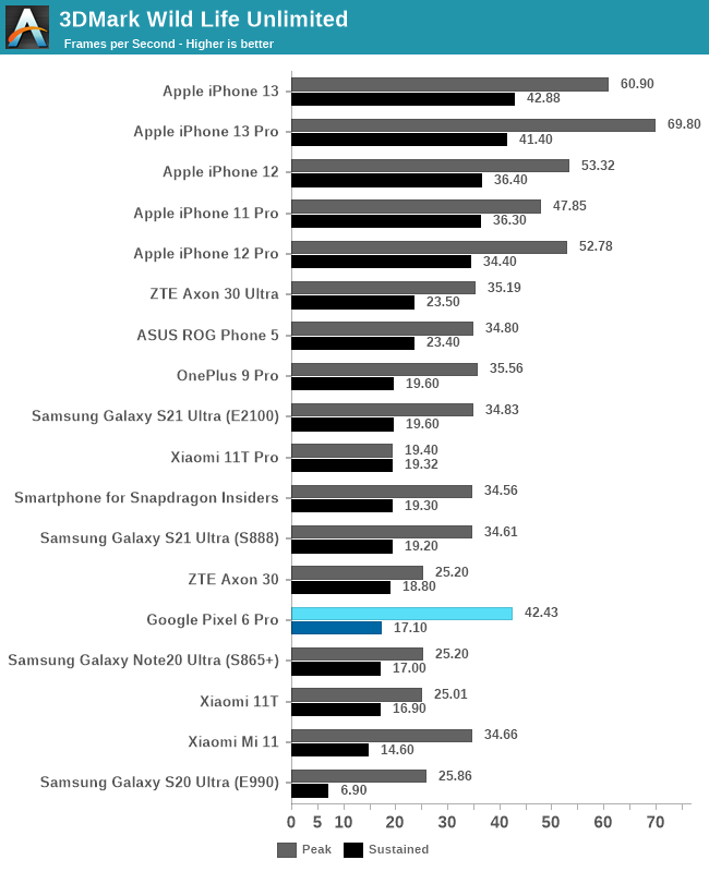
In 3DMark Wild Life unlimited, the first thing to note is that for some reason the regular Pixel 6 didn’t want to run the test as it errored out due to memory – I’m not sure what happened here, but it was isolated to the baseline model as the Pro unit had no issues.
The Pixel 6 Pro’s peak performance is respectable, however it’s only 21% faster than the Exynos 2100, not exactly what we’d expect from 21% more cores. A large issue with Mali GPUs of late has been that while you can throw more shader cores at the issue, the shared resources such as the tiler and L2 still remain as a single unit on the GPU. The G78’s ability to clock this part of the GPU higher is taken advantage of by Google in the Tensor implementation of the GPU, however that’s only 16% faster in pure clock frequency – maybe the workload is bottlenecked somewhere in this part of the GPU architecture.
Sustained performance off the start doesn’t look too good for the Pixel 6 Pro as it throttles considerably once the device gets hot, more on this in a bit.
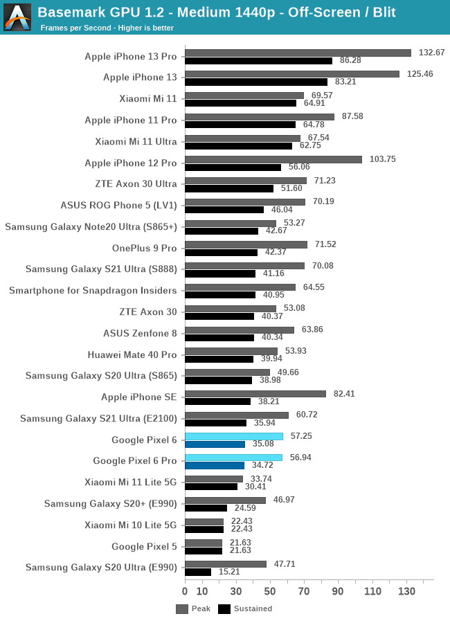
In Basemark GPU, the Pixel 6 phones both showcase odd peak performance figures that are way lower than we expected, here the chip doesn’t even manage to outperform the Exynos 2100. I’m not sure what the technical explanation here is, as on paper, the chip should be faster.
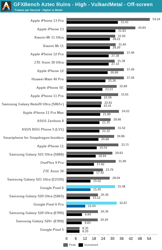
In Aztec High, the peak performance of the Tensor is again below what you’d expect, at +14% vs the Exynos 2100, and slightly ahead of the Snapdragon 888.
Sustained performance is quite bad here, and especially the Pixel 6 Pro seems to be running more severe throttling than the Pixel 6.
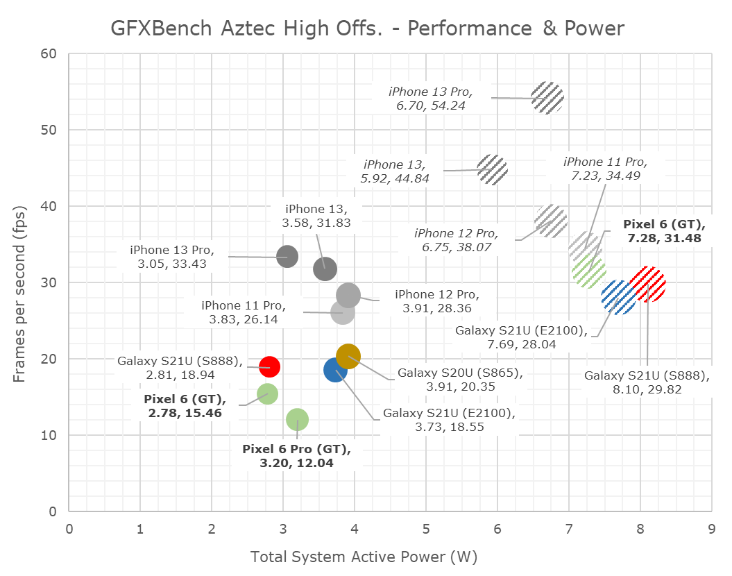
Looking at the power consumption of the phones, at peak performance, the Pixel 6 lands in around 7.28W, however this figure is a bit misleading. In actuality, the phone is running peak power figures in excess of 9-10W, but this is so much power, that the SoC isn’t able to complete a single run of the benchmark without throttling, so average power for a given run is actually much lower. This would also explain as to why our peak performance figures are less than what’s expected of a GPU clocked this high, it simply can’t maintain that speed for long enough to give off an FPS figure at the peak frequencies.
At sustained frequencies, the Pixel 6 and Pixel 6 Pro end up with different spots, however both are at quite low power figures around 3W.
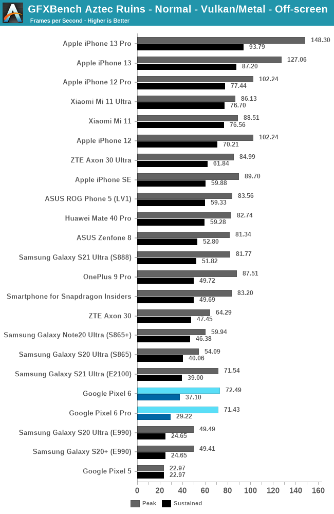
Aztec normal shows similar results, peak performance of the GPU is barely any better than the smaller configuration Exynos 2100 unit, and sustained performance figures are also significantly lower.
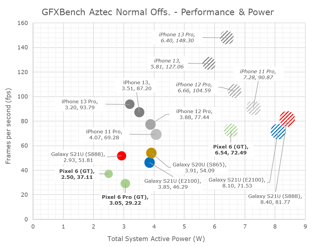
Sustained power after throttling on the phones is also quite weird here, as the phone seemingly throttles to <3W on the SoC. The Pixel 6 for some reason appears to have better power characteristics, it’s possible that chip bin has lower power than my 6 Pro unit.
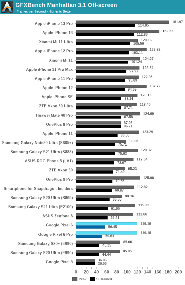
Manhattan 3.1 shows a similar peak and sustained performance standing, which isn’t too favourable for the Tensor.
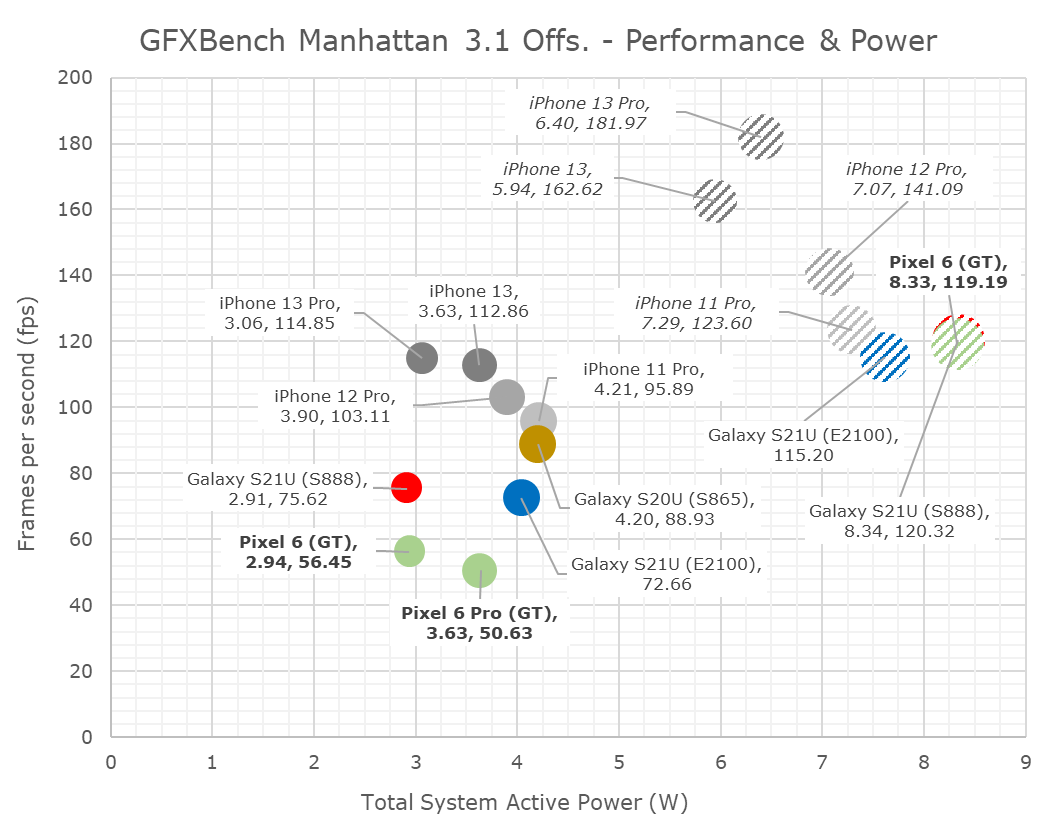
Power levels in Manhattan are higher than the Aztec benchmarks, I think the CPUs, or the DRAM contribute to more of the power due to the higher achieved framerates, and it slightly helps the heat dissipation rather than having everything focused on the GPU.
Overall, the GPU performance of the Google Tensor is quite disappointing. On paper, the massive G78MP20 GPU seemed like a juggernaut at the frequencies Google delivers the chip in, but in practice, it doesn’t reach the theoretical levels of performance. That being said, over the last year of SoC releases, almost every vendor in the industry has introduced some absurd ultra-high-power GPU configuration that throttles quickly. Why they do this, I don’t know, GPU compute for burst performance is always one of the reasons given, so maybe Google is also aiming the GPU towards compute rather than gaming.
In terms of sustained performance levels, the larger GPU in theory should have allowed it to run at lower frequencies, thus at better efficiency, and in turn deliver more performance than a smaller implementation like that of the Exynos 2100. The reality here is that the Pixel 6 phones struggle with thermal dissipation, and it’s something that seems to be completely unrelated to the chip itself.
Source: PBKreviews
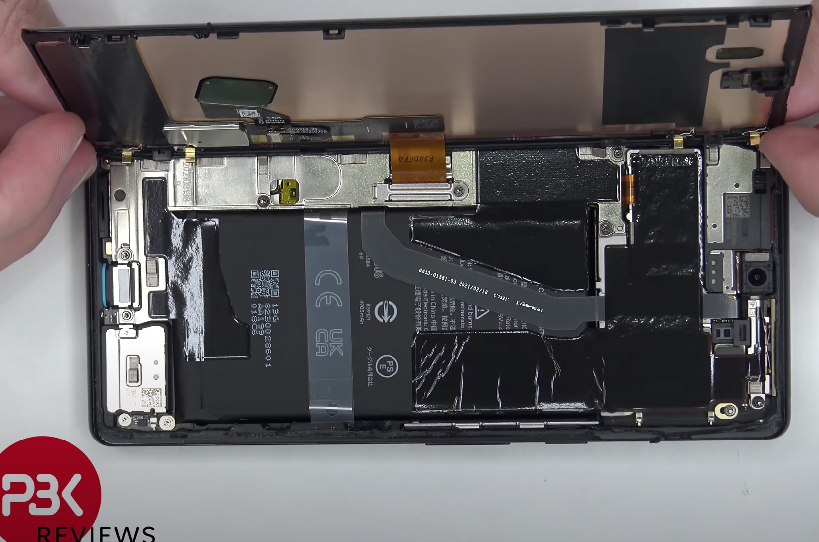
Both the Pixel 6 and Pixel 6 Pro are quite special in their hardware designs, in that they’re one of the rare Android devices out there which adopt an internal hardware design which doesn’t have a midframe adhered to the display panel. Looking at various teardowns of the phone, we can see that the display is relatively easily removable from the rest of the phone body, a design that’s actually more similar to Apple’s iPhones than any other Android flagship. This bodes well for the repairability of the screen, but it doesn’t do well for the thermal dissipation of the SoC. Much like iPhones have issues with thermal dissipation, and having much lower sustained power levels under stress, the Pixel 6 phones also suffer from the same issue as they cannot effectively use the display panel as a heat sink. This comes in contrast with other flagship Android devices – the Galaxy S21 Ultra for example has its display panel adhered to the midframe of the phone, it's not great for repairability, but it allows Samsung to employ a gigantic thermal dissipation pad the size of half of the phone footprint, with a direct heat pathway from the SoC to the display. Other thermally optimised devices out there share similar designs, able to better dump heat onto the full body of the phone.
The Pixel 6 Pro in contrast, has quite stark heat spots, with the left side of the phone, near the SoC, getting quite hot at up to 45°C, but at the same time the right side of the device here barely reaches 30-33°C, which is a large temperature gradient and signifies bad heat transfer abilities. Also, while I’m not sure how other people feel about this, but it does make the Pixel 6 phones feel more “hollow” in their build quality, but that might just be a nit-pick.
In any case, the Google Tensor’s chip gaming performance might be adequate, it’s no better than the Exynos 2100, and it gets further handicapped by the thermal design of the Pixel 6 phones. Generally, one can say it’s not the best phone for high-end gaming, which lines up with the subjective experiences with the devices in actual gaming demanding games like Genshin Impact.


108 Comments
View All Comments
Speedfriend - Thursday, November 4, 2021 - link
The average laptop costs $500 and most expensive laptops are bought by enterprises where Mac OS has a limited share. While the Macbookz are great devices, they are hobbled by poor monitor support at the Air end and cray prices at the MacBook Pro end. For most users the difference between the performance of a MacBook Pro and a $1000 laptop is unnoticeable except in their wallet!dukhawk - Tuesday, November 2, 2021 - link
The chip is very Exynos design related. Looking through the kernel source and there are a ton of Exynos named files.dukhawk - Tuesday, November 2, 2021 - link
https://android.googlesource.com/device/google/rav...defaultluser - Tuesday, November 2, 2021 - link
If anyone wants to know know why Nvidia is most interested in purchasing ARM, it's in order to put the inefficient Mali out of it's misery - and simultaneously replace it with their own license-able Geforce cores!Since ARM Corp started throwing in the GPU for free, they've had to cut GPU research (to pay for the increasingly complex CPU cores, all of which come out of the same revenue box!) But Nvidia has the massive Server Revenue to handle this architecture-design mismatch; they will keep the top 50% of the engineers, and cut the other cruft loose!
melgross - Tuesday, November 2, 2021 - link
That may be a side effect. But the reason for purchasing g it would be maki g money, and controlling the market. Yes, it’s true that Nvidia wa t to control all graphics and to turn the GPU into the main programming aim.TheinsanegamerN - Tuesday, November 2, 2021 - link
If nvidia wanted to do that they could simply license ARM and make their own superior chip. The fact they have fallen flat on their face every time they have tried speaks volumes.they want ARM for patents and $$$, nothing more.
defaultluser - Wednesday, November 3, 2021 - link
When a place like Rockchip can sell an Arm chip bundled with Mali for Peanuts, you can understand why superior GPU wasn't enough to win Phone customers!You also need integrated modem if you ever want to compete with Qualcomm (not something Nvidia was willing to do).
But that bundling system has been shorting ARM Mali development for years (Qualcomm, Apple, and soon Samsung (via AMD) are all bringing better high-end options into the field - you know your performance/watt must be pathetic when a company like Samsung is getting desperate-enough to pay the cost of porting AMD GPU over to ARM architecture.
Kvaern1 - Sunday, November 7, 2021 - link
"If nvidia wanted to do that they could simply license ARM and make their own superior chip."''simply'
No, no one can simply do that anymore and only two companies can. NVidia just bought one of them.
melgross - Tuesday, November 2, 2021 - link
I’m wondering about several things here.I don’t see the reason for using the A76 cores being one of time. This is a very new chip. The competitors on the Android side have been out for a while. They use A78 cores. Samsung uses A78 cores. So time doesn’t seem to be the issuer here, after all it does use the X1. So I wonder if it isn’t the size of the core on this already large, crowded chip that’s a reason, and possibly cost. If the newer cores take up more area they would cost slightly more. These chips are going to be bought in a fairly small number. Estimates have it that last year, Google sold between 4 and 7 million phones, and that they’re doubling this year’s order. Either would still be small, and give no advantage to Google in volume pricing compared to other chip makers.
The second is that you have to wonder if Google is following the Apple road here. Apple, of course, designs many chips, all for their own use. Will Google keep their chips for their own use, assuming they’re as successful in selling phones as Google hopes, or will they, after another generation, or two, when the chip is more of their own IP, offer them to other Android phone makers, and if so, how will Samsung feel about that, assuming their contract allows it?
SonOfKratos - Tuesday, November 2, 2021 - link
I think they went for the A76 cores because of cost, like you said Tensor is already huge and the A78 or A77 cores would be more power efficient but they are also much bigger than the A76 on 5nm process. Even if they were to clock an A78 lower it would just be a waste of money and space on the chip for them. They probably had a specific budget for the chip which meant a specific die size. This is not Apple who is willing to throw as much money as they can to get the best performance per watt.The display was rumored to be an E5 display from Samsung display which is in their latest display so I don't know why Google is not pushing for higher brightness but it could be because of heat dissipation as well...I highly doubt Samsung gave Google their garbage displays lol Also Google does not utilize the variable refresh rate very well and it's terrible for battery life. I have also seen a lot of janky scrolling with 120Hz in apps like Twitter..it has hiccups scrolling through the timeline compared to my Pixel 3.
The modem is very interesting probably more so than Tensor, this is the first competition for Qualcomm in the US at least. A lot of people have been saying that the modem is integrated in Tensor but why would Google integrate a modem that does not belong to them in "their" chip? That's like asking Apple to integrate Qualcomm modems in their chip. Also Samsung pays Qualcomm royalties for 5G so they probably have a special agreement surrounding the sale and implementation of the modem. It is definitely not as power efficient as Qualcomm's implementation but it's Good start. I got 400+ Mbps on T-Mobile 5GUC outdoors and 200 Mbps indoors (I don't know which band). It surprisingly supports n258 band like the iPhone.