Google's Tensor inside of Pixel 6, Pixel 6 Pro: A Look into Performance & Efficiency
by Andrei Frumusanu on November 2, 2021 8:00 AM EST- Posted in
- Mobile
- Smartphones
- SoCs
- Pixel 6
- Pixel 6 Pro
- Google Tensor
CPU Performance & Power
On the CPU side of things, the Tensor SoC, as we discussed, does have some larger configuration differences to what we’ve seen on the Exynos 2100, and is actually more similar to the Snapdragon 888 in that regard, at least from the view of a single Cortex-X1 cores. Having double the L2 cache, however being clocked 3.7%, or 110MHz lower, the Tensor and the Exynos should perform somewhat similarly, but dependent on the workload. The Snapdragon 888 showcases much better memory latency, so let’s also see if that actually plays out as such in the workloads.

In the individual subtests in the SPEC suite, the Tensor fares well and at first glance isn’t all too different from the other two competitor SoCs, albeit there are changes, and there are some oddities in the performance metrics.
Pure memory latency workloads as expected seem to be a weakness of the chip (within what one call weakness given the small differences between the different chips). 505.mcf_r falls behind the Exynos 2100 by a small amount, the doubled L2 cache should have made more of a difference here in my expectations, also 502.gcc_r should have seen larger benefits but they fail to materialise. 519.lbm_r is bandwidth hungry and here it seems the chip does have a slight advantage, but power is still extremely high and pretty much in line with the Exynos 2100, quite higher than the Snapdragon 888.
531.deepsjeng is extremely low – I’ve seen this behaviour in another SoC, the Dimensity 1200 inside the Xiaomi 11T, and this was due to the memory controllers and DRAM running slower than intended. I think we’re seeing the same characteristic here with the Tensor as its way of controlling the memory controller frequency via CPU memory stall counters doesn’t seem to be working well in this workload. 557.xz_r is also below expectations, being 18% slower than the Snapdragon 888, and ending up using also more energy than both Exynos and Snapdragon. I remember ex-Arm’s Mike Filippo once saying that every single clock cycle the core is wasting on waiting on memory has bad effects on performance and efficiency and it seems that’s what’s happening here with the Tensor and the way it controls memory.
In more execution bound workloads, in the int suite the Tensor does well in 525.x264 which I think is due to the larger L2. On the FP suite, we’re seeing some weird results, especially on the power side. 511.povray appears to be using a non-significant amount lesser power than the Exynos 2100 even though performance is identical. 538.imagick also shows much less power usage on the part of the Tensor, at similar performance. Povray might benefit from the larger L2 and lower operating frequency (less voltage, more efficiency), but I can’t really explain the imagick result – in general the Tensor SoC uses quite less power in all the FP workloads compared to the Exynos, while this difference isn’t as great in the INT workloads. Possibly the X1 cores have some better physical implementation on the Tensor chip which reduces the FP power.

In the aggregate scores, the Tensor / GS101 lands slightly worse in performance than the Exynos 2100, and lags behind the Snapdragon 888 by a more notable 12.2% margin, all whilst consuming 13.8% more energy due to completing the task slower. The performance deficit against the Snapdragon should really only be 1.4% - or a 40MHz difference, so I’m attributing the loss here just to the way Google runs their memory, or maybe also to possible real latency disadvantages of the SoC fabric. In SPECfp, which is more memory bandwidth sensitive (at least in the full suite, less so in our C/C++ subset), the Tensor SoC roughly matches the Snapdragon and Exynos in performance, while power and efficiency is closer to the Snapdragon, using 11.5% less power than the Exynos, and thus being more efficient here.
One issue that I encountered with the Tensor, that marks it being extremely similar in behaviour to the Exynos 2100, is throttling on the X1 cores. Notably, the Exynos chip had issues running its cores at their peak freq in active cooling under room temperature (~23°C) – the Snapdragon 888 had no such issues. I’m seeing similar behaviour on the Google Tensor’s X1 cores, albeit not as severe. The phone notably required sub-ambient cooling (I tested at 11°C) to get sustained peak frequencies, scoring 5-9% better, particularly on the FP subtests.
I’m skipping over the detailed A76 and A55 subscores of the Tensor as it’s not that interesting, however the aggregate scores are something we must discuss. As alluded to in the introduction, Google’s choice of using an A76 in the chip seemed extremely hard to justify, and the practical results we’re seeing the testing pretty much confirm our bad expectations of this CPU. The Tensor is running the A76 at 2.25GHz. The most similar data-point in the chart is the 2.5GHz A76 cores of the Exynos 990 – we have to remember this was an 7LPP SoC while the Tensor is a 5LPE design like the Eynos 2100 and Snapdraogn 888.
The Tensor’s A76 ends up more efficient than the Exynos 990’s – would would hope this to be the case, however when looking at the Snapdragon 888’s A78 cores which perform a whopping 46% better while using less energy to do so, it makes the Tensor’s A76 mid-cores look extremely bad. The IPC difference between the two chips is indeed around 34%, which is in line with the microarchitectural gap between the A76 and A78. The Tensor’s cores use a little bit less absolute power, but if this was Google top priority, they could have simply clocked a hypothetical A78 lower as well, and still ended up with a more performant and more efficient CPU setup. All in all, we didn’t understand why Google chose A76’s, as all the results end up expectedly bad, with the only explanation simply being that maybe Google just didn’t have a choice here, and just took whatever Samsung could implement.
On the side of the Cortex-A55 cores, things also aren’t looking fantastic for the Tensor SoC. The cores do end up performing the equally clocked A55’s of the Snapdragon 888 by 11% - maybe due to the faster L3 access, or access to the chip’s SLC, however efficiency here just isn’t good, as it uses almost double the power, and is more characteristic of the higher power levels of the Exynos chips’ A55 cores. It’s here where I come back to say that what makes a SoC from one vendor different to the SoC from another is the very foundations and fabric design - for the low-power A55 cores of the Tensor, the architecture of the SoC encounters the same issues of being overshadowed in system power, same as we see on Exynos chips, ending up in power efficiency that’s actually quite worse than the same chips own A76 cores, and much worse than the Snapdragon 888. MediaTek’s Dimensity 1200 even goes further in operating their chip in seemingly the most efficient way for their A55 cores, not to mention Apple’s SoCs.
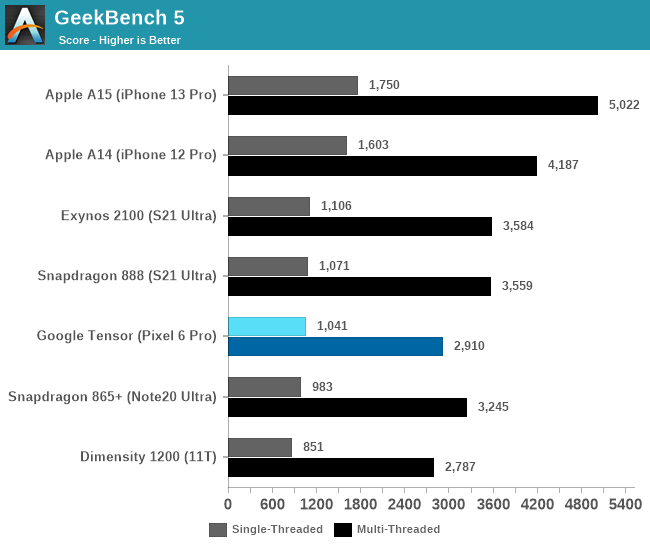
While we don’t run multi-threaded SPEC on phones, we can revert back to GeekBench 5 which serves the purpose very well.
Although the Google Tensor has double as many X1 cores as the other Android SoCs, the fact that the Cortex-A76 cores underperform by such a larger degree the middle cores of the competition, means that the total sum of MT performance of the chip is lesser than that of the competition.
Overall, the Google Tensor’s CPU setup, performance, and efficiency is a mixed bag. The two X1 cores of the chip end up slightly slower than the competition, and efficiency is most of the time in line with the Exynos 2100’s X1 cores – sometimes keeping up with the Snapdragon 888 in some workloads. The Cortex-A76 middle cores of the chip in my view make no sense, as their performance and energy efficiency just aren’t up to date with 2021 designs. Finally, the A55 behavioural characteristic showcases that this chip is very much related to Samsung’s Exynos SoCs, falling behind in efficiency compared to how Qualcomm or MediaTek are able to operate their SoCs.


108 Comments
View All Comments
Speedfriend - Thursday, November 4, 2021 - link
The average laptop costs $500 and most expensive laptops are bought by enterprises where Mac OS has a limited share. While the Macbookz are great devices, they are hobbled by poor monitor support at the Air end and cray prices at the MacBook Pro end. For most users the difference between the performance of a MacBook Pro and a $1000 laptop is unnoticeable except in their wallet!dukhawk - Tuesday, November 2, 2021 - link
The chip is very Exynos design related. Looking through the kernel source and there are a ton of Exynos named files.dukhawk - Tuesday, November 2, 2021 - link
https://android.googlesource.com/device/google/rav...defaultluser - Tuesday, November 2, 2021 - link
If anyone wants to know know why Nvidia is most interested in purchasing ARM, it's in order to put the inefficient Mali out of it's misery - and simultaneously replace it with their own license-able Geforce cores!Since ARM Corp started throwing in the GPU for free, they've had to cut GPU research (to pay for the increasingly complex CPU cores, all of which come out of the same revenue box!) But Nvidia has the massive Server Revenue to handle this architecture-design mismatch; they will keep the top 50% of the engineers, and cut the other cruft loose!
melgross - Tuesday, November 2, 2021 - link
That may be a side effect. But the reason for purchasing g it would be maki g money, and controlling the market. Yes, it’s true that Nvidia wa t to control all graphics and to turn the GPU into the main programming aim.TheinsanegamerN - Tuesday, November 2, 2021 - link
If nvidia wanted to do that they could simply license ARM and make their own superior chip. The fact they have fallen flat on their face every time they have tried speaks volumes.they want ARM for patents and $$$, nothing more.
defaultluser - Wednesday, November 3, 2021 - link
When a place like Rockchip can sell an Arm chip bundled with Mali for Peanuts, you can understand why superior GPU wasn't enough to win Phone customers!You also need integrated modem if you ever want to compete with Qualcomm (not something Nvidia was willing to do).
But that bundling system has been shorting ARM Mali development for years (Qualcomm, Apple, and soon Samsung (via AMD) are all bringing better high-end options into the field - you know your performance/watt must be pathetic when a company like Samsung is getting desperate-enough to pay the cost of porting AMD GPU over to ARM architecture.
Kvaern1 - Sunday, November 7, 2021 - link
"If nvidia wanted to do that they could simply license ARM and make their own superior chip."''simply'
No, no one can simply do that anymore and only two companies can. NVidia just bought one of them.
melgross - Tuesday, November 2, 2021 - link
I’m wondering about several things here.I don’t see the reason for using the A76 cores being one of time. This is a very new chip. The competitors on the Android side have been out for a while. They use A78 cores. Samsung uses A78 cores. So time doesn’t seem to be the issuer here, after all it does use the X1. So I wonder if it isn’t the size of the core on this already large, crowded chip that’s a reason, and possibly cost. If the newer cores take up more area they would cost slightly more. These chips are going to be bought in a fairly small number. Estimates have it that last year, Google sold between 4 and 7 million phones, and that they’re doubling this year’s order. Either would still be small, and give no advantage to Google in volume pricing compared to other chip makers.
The second is that you have to wonder if Google is following the Apple road here. Apple, of course, designs many chips, all for their own use. Will Google keep their chips for their own use, assuming they’re as successful in selling phones as Google hopes, or will they, after another generation, or two, when the chip is more of their own IP, offer them to other Android phone makers, and if so, how will Samsung feel about that, assuming their contract allows it?
SonOfKratos - Tuesday, November 2, 2021 - link
I think they went for the A76 cores because of cost, like you said Tensor is already huge and the A78 or A77 cores would be more power efficient but they are also much bigger than the A76 on 5nm process. Even if they were to clock an A78 lower it would just be a waste of money and space on the chip for them. They probably had a specific budget for the chip which meant a specific die size. This is not Apple who is willing to throw as much money as they can to get the best performance per watt.The display was rumored to be an E5 display from Samsung display which is in their latest display so I don't know why Google is not pushing for higher brightness but it could be because of heat dissipation as well...I highly doubt Samsung gave Google their garbage displays lol Also Google does not utilize the variable refresh rate very well and it's terrible for battery life. I have also seen a lot of janky scrolling with 120Hz in apps like Twitter..it has hiccups scrolling through the timeline compared to my Pixel 3.
The modem is very interesting probably more so than Tensor, this is the first competition for Qualcomm in the US at least. A lot of people have been saying that the modem is integrated in Tensor but why would Google integrate a modem that does not belong to them in "their" chip? That's like asking Apple to integrate Qualcomm modems in their chip. Also Samsung pays Qualcomm royalties for 5G so they probably have a special agreement surrounding the sale and implementation of the modem. It is definitely not as power efficient as Qualcomm's implementation but it's Good start. I got 400+ Mbps on T-Mobile 5GUC outdoors and 200 Mbps indoors (I don't know which band). It surprisingly supports n258 band like the iPhone.