Google's Tensor inside of Pixel 6, Pixel 6 Pro: A Look into Performance & Efficiency
by Andrei Frumusanu on November 2, 2021 8:00 AM EST- Posted in
- Mobile
- Smartphones
- SoCs
- Pixel 6
- Pixel 6 Pro
- Google Tensor
GPU Performance & Power
The Google Tensors GPU is quite a beast. A Mali G78 with 20 cores, it’s sporting 42% more cores than the Exynos 2100 implementation, and only comes second after HiSilicon’s Kirin 9000. However, unlike the more power efficient N5 process node of the Kirin 9000, the Tensor SoC comes on the same process node as on the Exynos 2100. Having a much larger GPU, one would expect Google to drive the block at lower frequencies, in order to achieve better energy efficiency. To our surprise, the G78MP20 runs at up to 1GHz on the tiler and L2, and up to 848MHz on the shader cores, which is essentially the same as the smaller Exynos 2100 implementation of the GPU. Of course this immediately raises red flags for the Tensor when it comes to power consumption, as the chip certainly can’t pull out a rabbit out of a hat in terms of efficiency, so let’s see what happens:
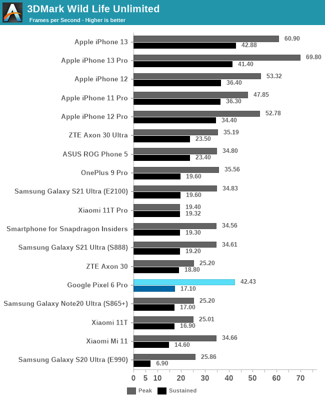
In 3DMark Wild Life unlimited, the first thing to note is that for some reason the regular Pixel 6 didn’t want to run the test as it errored out due to memory – I’m not sure what happened here, but it was isolated to the baseline model as the Pro unit had no issues.
The Pixel 6 Pro’s peak performance is respectable, however it’s only 21% faster than the Exynos 2100, not exactly what we’d expect from 21% more cores. A large issue with Mali GPUs of late has been that while you can throw more shader cores at the issue, the shared resources such as the tiler and L2 still remain as a single unit on the GPU. The G78’s ability to clock this part of the GPU higher is taken advantage of by Google in the Tensor implementation of the GPU, however that’s only 16% faster in pure clock frequency – maybe the workload is bottlenecked somewhere in this part of the GPU architecture.
Sustained performance off the start doesn’t look too good for the Pixel 6 Pro as it throttles considerably once the device gets hot, more on this in a bit.
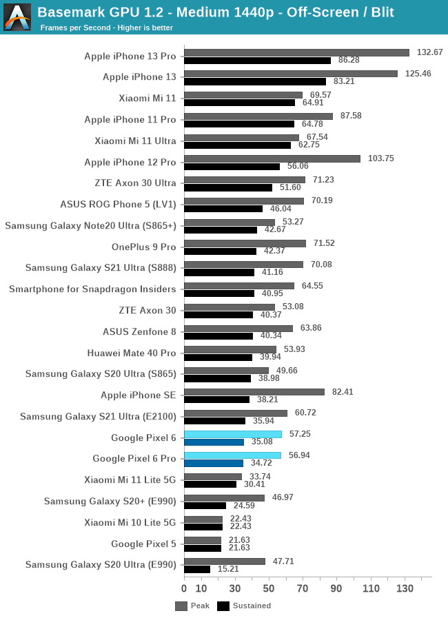
In Basemark GPU, the Pixel 6 phones both showcase odd peak performance figures that are way lower than we expected, here the chip doesn’t even manage to outperform the Exynos 2100. I’m not sure what the technical explanation here is, as on paper, the chip should be faster.
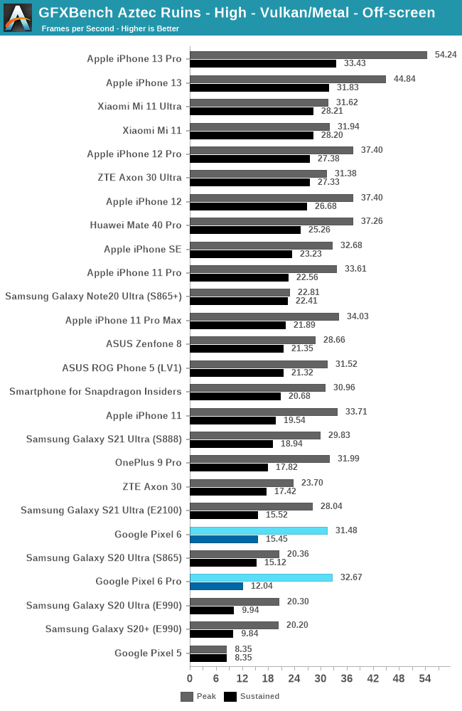
In Aztec High, the peak performance of the Tensor is again below what you’d expect, at +14% vs the Exynos 2100, and slightly ahead of the Snapdragon 888.
Sustained performance is quite bad here, and especially the Pixel 6 Pro seems to be running more severe throttling than the Pixel 6.
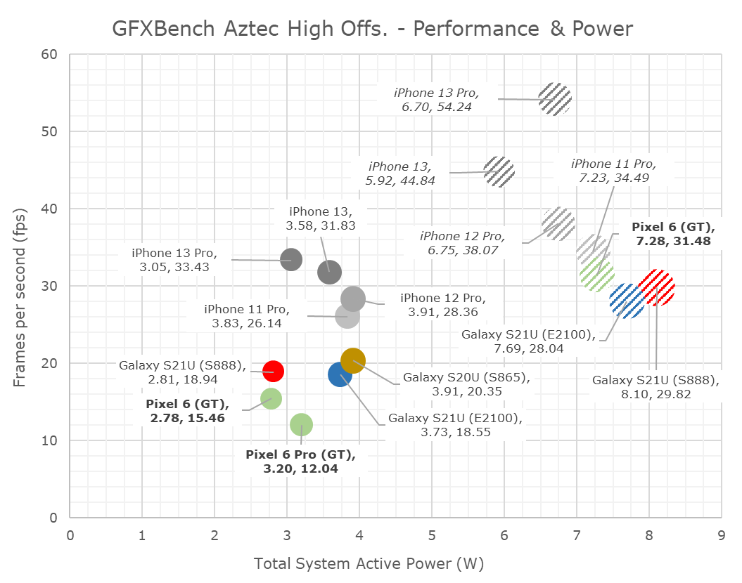
Looking at the power consumption of the phones, at peak performance, the Pixel 6 lands in around 7.28W, however this figure is a bit misleading. In actuality, the phone is running peak power figures in excess of 9-10W, but this is so much power, that the SoC isn’t able to complete a single run of the benchmark without throttling, so average power for a given run is actually much lower. This would also explain as to why our peak performance figures are less than what’s expected of a GPU clocked this high, it simply can’t maintain that speed for long enough to give off an FPS figure at the peak frequencies.
At sustained frequencies, the Pixel 6 and Pixel 6 Pro end up with different spots, however both are at quite low power figures around 3W.
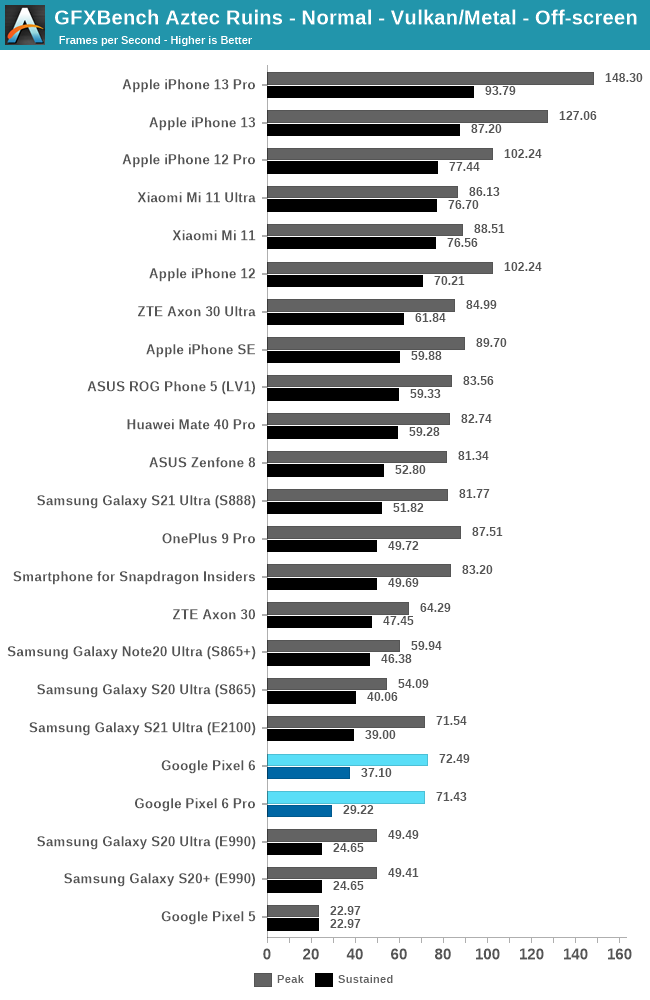
Aztec normal shows similar results, peak performance of the GPU is barely any better than the smaller configuration Exynos 2100 unit, and sustained performance figures are also significantly lower.
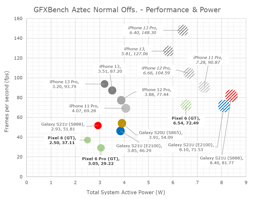
Sustained power after throttling on the phones is also quite weird here, as the phone seemingly throttles to <3W on the SoC. The Pixel 6 for some reason appears to have better power characteristics, it’s possible that chip bin has lower power than my 6 Pro unit.
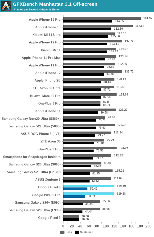
Manhattan 3.1 shows a similar peak and sustained performance standing, which isn’t too favourable for the Tensor.
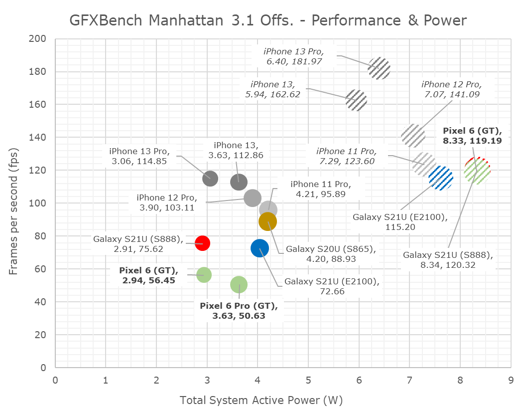
Power levels in Manhattan are higher than the Aztec benchmarks, I think the CPUs, or the DRAM contribute to more of the power due to the higher achieved framerates, and it slightly helps the heat dissipation rather than having everything focused on the GPU.
Overall, the GPU performance of the Google Tensor is quite disappointing. On paper, the massive G78MP20 GPU seemed like a juggernaut at the frequencies Google delivers the chip in, but in practice, it doesn’t reach the theoretical levels of performance. That being said, over the last year of SoC releases, almost every vendor in the industry has introduced some absurd ultra-high-power GPU configuration that throttles quickly. Why they do this, I don’t know, GPU compute for burst performance is always one of the reasons given, so maybe Google is also aiming the GPU towards compute rather than gaming.
In terms of sustained performance levels, the larger GPU in theory should have allowed it to run at lower frequencies, thus at better efficiency, and in turn deliver more performance than a smaller implementation like that of the Exynos 2100. The reality here is that the Pixel 6 phones struggle with thermal dissipation, and it’s something that seems to be completely unrelated to the chip itself.
Source: PBKreviews
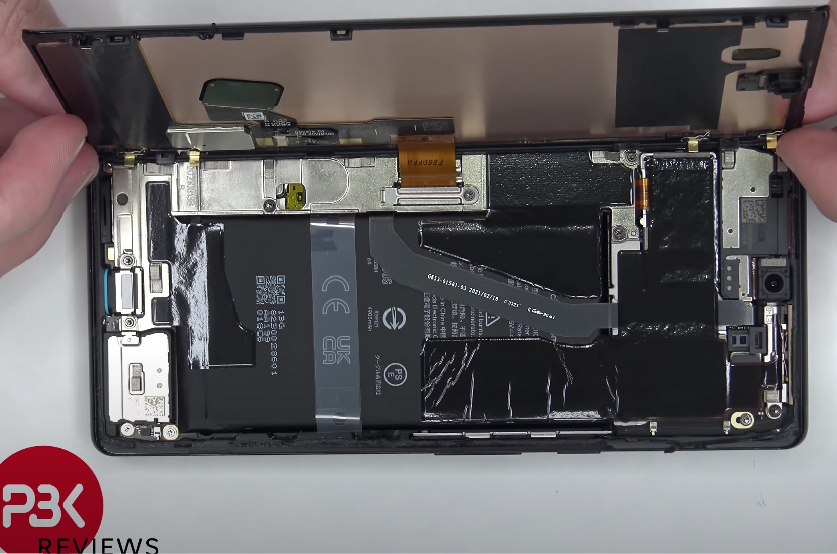
Both the Pixel 6 and Pixel 6 Pro are quite special in their hardware designs, in that they’re one of the rare Android devices out there which adopt an internal hardware design which doesn’t have a midframe adhered to the display panel. Looking at various teardowns of the phone, we can see that the display is relatively easily removable from the rest of the phone body, a design that’s actually more similar to Apple’s iPhones than any other Android flagship. This bodes well for the repairability of the screen, but it doesn’t do well for the thermal dissipation of the SoC. Much like iPhones have issues with thermal dissipation, and having much lower sustained power levels under stress, the Pixel 6 phones also suffer from the same issue as they cannot effectively use the display panel as a heat sink. This comes in contrast with other flagship Android devices – the Galaxy S21 Ultra for example has its display panel adhered to the midframe of the phone, it's not great for repairability, but it allows Samsung to employ a gigantic thermal dissipation pad the size of half of the phone footprint, with a direct heat pathway from the SoC to the display. Other thermally optimised devices out there share similar designs, able to better dump heat onto the full body of the phone.
The Pixel 6 Pro in contrast, has quite stark heat spots, with the left side of the phone, near the SoC, getting quite hot at up to 45°C, but at the same time the right side of the device here barely reaches 30-33°C, which is a large temperature gradient and signifies bad heat transfer abilities. Also, while I’m not sure how other people feel about this, but it does make the Pixel 6 phones feel more “hollow” in their build quality, but that might just be a nit-pick.
In any case, the Google Tensor’s chip gaming performance might be adequate, it’s no better than the Exynos 2100, and it gets further handicapped by the thermal design of the Pixel 6 phones. Generally, one can say it’s not the best phone for high-end gaming, which lines up with the subjective experiences with the devices in actual gaming demanding games like Genshin Impact.


108 Comments
View All Comments
anonym - Sunday, November 7, 2021 - link
I don't have any data but A76 is more efficient than A78 while relatively lower performance region. According to following DVFS carves, A77 is out of the question.https://images.anandtech.com/doci/15813/A78-X1-cro...
boozed - Tuesday, November 2, 2021 - link
So do we call this design "semi-custom" or "very-slightly-custom"?watzupken - Wednesday, November 3, 2021 - link
I think we have come to a point that pushing performance for mobile devices is starting to slow down big time, or in some cases like Exynos where we see regressions. The SOC gets refreshed each year, pushing for higher performance. The fabs however is slower to catch up, and despite the marketing of 7nm, 5nm, 3nm, etc, they may not be anywhere near what is being marketed. In this case, squeezing a fat GPU sounds great on paper, but in real life, the sustained performance is not going to make a huge difference because of the power and heat. In any case, I feel the push for an annual SOC upgrade should slow down because I certainly don't see significant difference in real life performance. We generally only know that last years SOCs are slower only when running benchmarks. Even in games, last gen high end SOCs can still handle challenging titles. Instead, they should focus on making the SOCs more power efficient.damianrobertjones - Wednesday, November 3, 2021 - link
All I want is for all phones to be able to record the front and rear camera at the same time. VLog fun. Such a simple thing... .Whiteknight2020 - Wednesday, November 3, 2021 - link
Not India, China, UK, Russia, most of the EU, Africa. Which is the vast majority of the world's population and the vast majority of the world's phones, a great many of which are still feature phones.Whiteknight2020 - Wednesday, November 3, 2021 - link
Not India, China, UK, Russia, most of the EU, Africa. Which is the vast majority of the world's population and the vast majority of the world's phones, a great many of which are still feature phones.eastcoast_pete - Wednesday, November 3, 2021 - link
To me, one of the most interesting points about this "meh" first Google custom SoC is that it was created with lots of Lego blocks from Samsung; I guess Google working with Qualcomm was either out of the question or not something either was willing to do. Maybe this was about Google wanting to show QC that they can develop a Pixel smartphone without them, maybe the two compete too closely on ML/AI, or maybe they just don't like each other much right now - who knows? Still, an SD 888-derived SoC with Google TPU would have likely been better on performance and efficiency. This one here is an odd duck. As for the Pixel 6, especially the Pro: camera is supposed to be spectacular, but with the battery life as it is and, of course (Google, after all), no expandable storage and no 3.5 mm headphone connectors, it missed the mark for me. But, the Pixels are sold out, so why would Google change?Whiteknight2020 - Wednesday, November 3, 2021 - link
If you want a "really excellent camera", sorry to disappoint you but you'll need to be buying an actual camera. The only thing a multipurpose portable computing device can ever be excellent at is being a multipurpose portable computing device.FunBunny2 - Wednesday, November 3, 2021 - link
"a multipurpose portable computing device."isn't that pretty much verbatim what Stevie said when he showed the original iPhone? nothing has really changed since. it was, kinda, a big deal when Stevie intoned that the thingee incorporated 3, count em 3!, devices that you had to carry that day!!! internet, phone, and number 3 (whatever that was). is a 2021 smartphone really anything more?? I mean, beyond the capacity of more transistors. thank ASML (and some really smart physicists and engineers) for that not Apple or Samsung or Google or ... last time I checked Apple's 'our own ARM' SoC is just bigger and wider ARM ISA, due to the, so far, increasing transistor budget available at the foundries.
that all begs the fundamental question: if Apple and The Seven Dwarfs have access to the same physical capital (ASML, et al) why the difference? if everybody spends time and money tweaking a function (that they all need, one way or another), in some time (short, I'll assert) The One Best Way emerges. the task, in the final analysis, is just maths. of course, Best is not a point estimate, as many comments make clear; there're trade offs all along the line.
it would be fun to use one of the Damn Gummint's supercomputers (weather or nucular bomb design) to spec a SoC. wonder how different the result would be?
NaturalViolence - Wednesday, November 3, 2021 - link
The math for the memory bandwidth doesn't check out. From the article:"4x 16-bit CH
@ 3200MHz LPDDR5 / 51.2GB/s"
But 3200MHz x 64 bit is 25.6GB/s, not 51.2GB/s. So which is it?