Google's Tensor inside of Pixel 6, Pixel 6 Pro: A Look into Performance & Efficiency
by Andrei Frumusanu on November 2, 2021 8:00 AM EST- Posted in
- Mobile
- Smartphones
- SoCs
- Pixel 6
- Pixel 6 Pro
- Google Tensor
CPU Performance & Power
On the CPU side of things, the Tensor SoC, as we discussed, does have some larger configuration differences to what we’ve seen on the Exynos 2100, and is actually more similar to the Snapdragon 888 in that regard, at least from the view of a single Cortex-X1 cores. Having double the L2 cache, however being clocked 3.7%, or 110MHz lower, the Tensor and the Exynos should perform somewhat similarly, but dependent on the workload. The Snapdragon 888 showcases much better memory latency, so let’s also see if that actually plays out as such in the workloads.

In the individual subtests in the SPEC suite, the Tensor fares well and at first glance isn’t all too different from the other two competitor SoCs, albeit there are changes, and there are some oddities in the performance metrics.
Pure memory latency workloads as expected seem to be a weakness of the chip (within what one call weakness given the small differences between the different chips). 505.mcf_r falls behind the Exynos 2100 by a small amount, the doubled L2 cache should have made more of a difference here in my expectations, also 502.gcc_r should have seen larger benefits but they fail to materialise. 519.lbm_r is bandwidth hungry and here it seems the chip does have a slight advantage, but power is still extremely high and pretty much in line with the Exynos 2100, quite higher than the Snapdragon 888.
531.deepsjeng is extremely low – I’ve seen this behaviour in another SoC, the Dimensity 1200 inside the Xiaomi 11T, and this was due to the memory controllers and DRAM running slower than intended. I think we’re seeing the same characteristic here with the Tensor as its way of controlling the memory controller frequency via CPU memory stall counters doesn’t seem to be working well in this workload. 557.xz_r is also below expectations, being 18% slower than the Snapdragon 888, and ending up using also more energy than both Exynos and Snapdragon. I remember ex-Arm’s Mike Filippo once saying that every single clock cycle the core is wasting on waiting on memory has bad effects on performance and efficiency and it seems that’s what’s happening here with the Tensor and the way it controls memory.
In more execution bound workloads, in the int suite the Tensor does well in 525.x264 which I think is due to the larger L2. On the FP suite, we’re seeing some weird results, especially on the power side. 511.povray appears to be using a non-significant amount lesser power than the Exynos 2100 even though performance is identical. 538.imagick also shows much less power usage on the part of the Tensor, at similar performance. Povray might benefit from the larger L2 and lower operating frequency (less voltage, more efficiency), but I can’t really explain the imagick result – in general the Tensor SoC uses quite less power in all the FP workloads compared to the Exynos, while this difference isn’t as great in the INT workloads. Possibly the X1 cores have some better physical implementation on the Tensor chip which reduces the FP power.

In the aggregate scores, the Tensor / GS101 lands slightly worse in performance than the Exynos 2100, and lags behind the Snapdragon 888 by a more notable 12.2% margin, all whilst consuming 13.8% more energy due to completing the task slower. The performance deficit against the Snapdragon should really only be 1.4% - or a 40MHz difference, so I’m attributing the loss here just to the way Google runs their memory, or maybe also to possible real latency disadvantages of the SoC fabric. In SPECfp, which is more memory bandwidth sensitive (at least in the full suite, less so in our C/C++ subset), the Tensor SoC roughly matches the Snapdragon and Exynos in performance, while power and efficiency is closer to the Snapdragon, using 11.5% less power than the Exynos, and thus being more efficient here.
One issue that I encountered with the Tensor, that marks it being extremely similar in behaviour to the Exynos 2100, is throttling on the X1 cores. Notably, the Exynos chip had issues running its cores at their peak freq in active cooling under room temperature (~23°C) – the Snapdragon 888 had no such issues. I’m seeing similar behaviour on the Google Tensor’s X1 cores, albeit not as severe. The phone notably required sub-ambient cooling (I tested at 11°C) to get sustained peak frequencies, scoring 5-9% better, particularly on the FP subtests.
I’m skipping over the detailed A76 and A55 subscores of the Tensor as it’s not that interesting, however the aggregate scores are something we must discuss. As alluded to in the introduction, Google’s choice of using an A76 in the chip seemed extremely hard to justify, and the practical results we’re seeing the testing pretty much confirm our bad expectations of this CPU. The Tensor is running the A76 at 2.25GHz. The most similar data-point in the chart is the 2.5GHz A76 cores of the Exynos 990 – we have to remember this was an 7LPP SoC while the Tensor is a 5LPE design like the Eynos 2100 and Snapdraogn 888.
The Tensor’s A76 ends up more efficient than the Exynos 990’s – would would hope this to be the case, however when looking at the Snapdragon 888’s A78 cores which perform a whopping 46% better while using less energy to do so, it makes the Tensor’s A76 mid-cores look extremely bad. The IPC difference between the two chips is indeed around 34%, which is in line with the microarchitectural gap between the A76 and A78. The Tensor’s cores use a little bit less absolute power, but if this was Google top priority, they could have simply clocked a hypothetical A78 lower as well, and still ended up with a more performant and more efficient CPU setup. All in all, we didn’t understand why Google chose A76’s, as all the results end up expectedly bad, with the only explanation simply being that maybe Google just didn’t have a choice here, and just took whatever Samsung could implement.
On the side of the Cortex-A55 cores, things also aren’t looking fantastic for the Tensor SoC. The cores do end up performing the equally clocked A55’s of the Snapdragon 888 by 11% - maybe due to the faster L3 access, or access to the chip’s SLC, however efficiency here just isn’t good, as it uses almost double the power, and is more characteristic of the higher power levels of the Exynos chips’ A55 cores. It’s here where I come back to say that what makes a SoC from one vendor different to the SoC from another is the very foundations and fabric design - for the low-power A55 cores of the Tensor, the architecture of the SoC encounters the same issues of being overshadowed in system power, same as we see on Exynos chips, ending up in power efficiency that’s actually quite worse than the same chips own A76 cores, and much worse than the Snapdragon 888. MediaTek’s Dimensity 1200 even goes further in operating their chip in seemingly the most efficient way for their A55 cores, not to mention Apple’s SoCs.
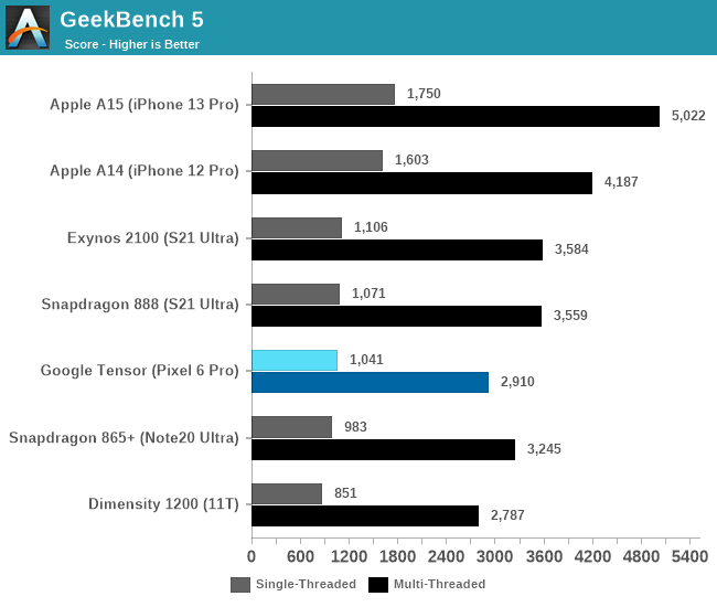
While we don’t run multi-threaded SPEC on phones, we can revert back to GeekBench 5 which serves the purpose very well.
Although the Google Tensor has double as many X1 cores as the other Android SoCs, the fact that the Cortex-A76 cores underperform by such a larger degree the middle cores of the competition, means that the total sum of MT performance of the chip is lesser than that of the competition.
Overall, the Google Tensor’s CPU setup, performance, and efficiency is a mixed bag. The two X1 cores of the chip end up slightly slower than the competition, and efficiency is most of the time in line with the Exynos 2100’s X1 cores – sometimes keeping up with the Snapdragon 888 in some workloads. The Cortex-A76 middle cores of the chip in my view make no sense, as their performance and energy efficiency just aren’t up to date with 2021 designs. Finally, the A55 behavioural characteristic showcases that this chip is very much related to Samsung’s Exynos SoCs, falling behind in efficiency compared to how Qualcomm or MediaTek are able to operate their SoCs.


108 Comments
View All Comments
anonym - Sunday, November 7, 2021 - link
I don't have any data but A76 is more efficient than A78 while relatively lower performance region. According to following DVFS carves, A77 is out of the question.https://images.anandtech.com/doci/15813/A78-X1-cro...
boozed - Tuesday, November 2, 2021 - link
So do we call this design "semi-custom" or "very-slightly-custom"?watzupken - Wednesday, November 3, 2021 - link
I think we have come to a point that pushing performance for mobile devices is starting to slow down big time, or in some cases like Exynos where we see regressions. The SOC gets refreshed each year, pushing for higher performance. The fabs however is slower to catch up, and despite the marketing of 7nm, 5nm, 3nm, etc, they may not be anywhere near what is being marketed. In this case, squeezing a fat GPU sounds great on paper, but in real life, the sustained performance is not going to make a huge difference because of the power and heat. In any case, I feel the push for an annual SOC upgrade should slow down because I certainly don't see significant difference in real life performance. We generally only know that last years SOCs are slower only when running benchmarks. Even in games, last gen high end SOCs can still handle challenging titles. Instead, they should focus on making the SOCs more power efficient.damianrobertjones - Wednesday, November 3, 2021 - link
All I want is for all phones to be able to record the front and rear camera at the same time. VLog fun. Such a simple thing... .Whiteknight2020 - Wednesday, November 3, 2021 - link
Not India, China, UK, Russia, most of the EU, Africa. Which is the vast majority of the world's population and the vast majority of the world's phones, a great many of which are still feature phones.Whiteknight2020 - Wednesday, November 3, 2021 - link
Not India, China, UK, Russia, most of the EU, Africa. Which is the vast majority of the world's population and the vast majority of the world's phones, a great many of which are still feature phones.eastcoast_pete - Wednesday, November 3, 2021 - link
To me, one of the most interesting points about this "meh" first Google custom SoC is that it was created with lots of Lego blocks from Samsung; I guess Google working with Qualcomm was either out of the question or not something either was willing to do. Maybe this was about Google wanting to show QC that they can develop a Pixel smartphone without them, maybe the two compete too closely on ML/AI, or maybe they just don't like each other much right now - who knows? Still, an SD 888-derived SoC with Google TPU would have likely been better on performance and efficiency. This one here is an odd duck. As for the Pixel 6, especially the Pro: camera is supposed to be spectacular, but with the battery life as it is and, of course (Google, after all), no expandable storage and no 3.5 mm headphone connectors, it missed the mark for me. But, the Pixels are sold out, so why would Google change?Whiteknight2020 - Wednesday, November 3, 2021 - link
If you want a "really excellent camera", sorry to disappoint you but you'll need to be buying an actual camera. The only thing a multipurpose portable computing device can ever be excellent at is being a multipurpose portable computing device.FunBunny2 - Wednesday, November 3, 2021 - link
"a multipurpose portable computing device."isn't that pretty much verbatim what Stevie said when he showed the original iPhone? nothing has really changed since. it was, kinda, a big deal when Stevie intoned that the thingee incorporated 3, count em 3!, devices that you had to carry that day!!! internet, phone, and number 3 (whatever that was). is a 2021 smartphone really anything more?? I mean, beyond the capacity of more transistors. thank ASML (and some really smart physicists and engineers) for that not Apple or Samsung or Google or ... last time I checked Apple's 'our own ARM' SoC is just bigger and wider ARM ISA, due to the, so far, increasing transistor budget available at the foundries.
that all begs the fundamental question: if Apple and The Seven Dwarfs have access to the same physical capital (ASML, et al) why the difference? if everybody spends time and money tweaking a function (that they all need, one way or another), in some time (short, I'll assert) The One Best Way emerges. the task, in the final analysis, is just maths. of course, Best is not a point estimate, as many comments make clear; there're trade offs all along the line.
it would be fun to use one of the Damn Gummint's supercomputers (weather or nucular bomb design) to spec a SoC. wonder how different the result would be?
NaturalViolence - Wednesday, November 3, 2021 - link
The math for the memory bandwidth doesn't check out. From the article:"4x 16-bit CH
@ 3200MHz LPDDR5 / 51.2GB/s"
But 3200MHz x 64 bit is 25.6GB/s, not 51.2GB/s. So which is it?