Arm Announces Mobile Armv9 CPU Microarchitectures: Cortex-X2, Cortex-A710 & Cortex-A510
by Andrei Frumusanu on May 25, 2021 9:00 AM EST- Posted in
- SoCs
- CPUs
- Arm
- Smartphones
- Mobile
- Cortex
- ARMv9
- Cortex-X2
- Cortex-A710
- Cortex-A510
New DSU-110 L3 & Cluster: Massively More Bandwidth
Alongside the new CPU microarchitectures, Arm today is also announcing a new L3 design in the form of the new DSU-110. The “DynamIQ Shared Unit” had been the company’s go-to cluster and “core complex” block ever since it was introduced in 2017 with the Cortex-A75 and Cortex-A55. While we’ve seen small iterative improvements, today’s DSU-110 marks a major change in how the DSU operates and how it promises to scale up in cache size and bandwidth.
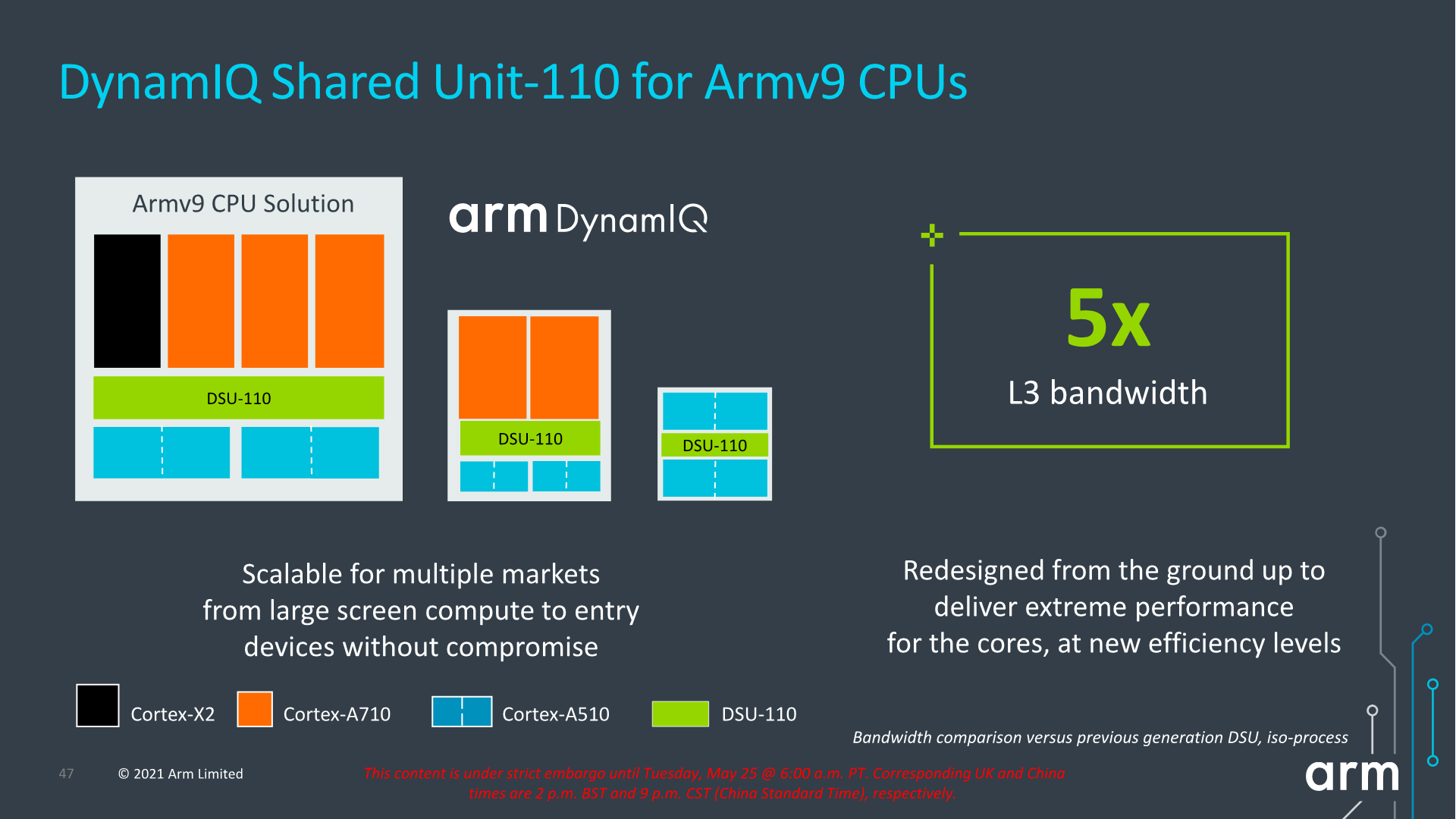
The new DSU-110 is a ground-up redesign with an emphasis on more bandwidth and more power efficiency. It continues to be the core building block for all of Arm’s mobile and lower tier market segments.
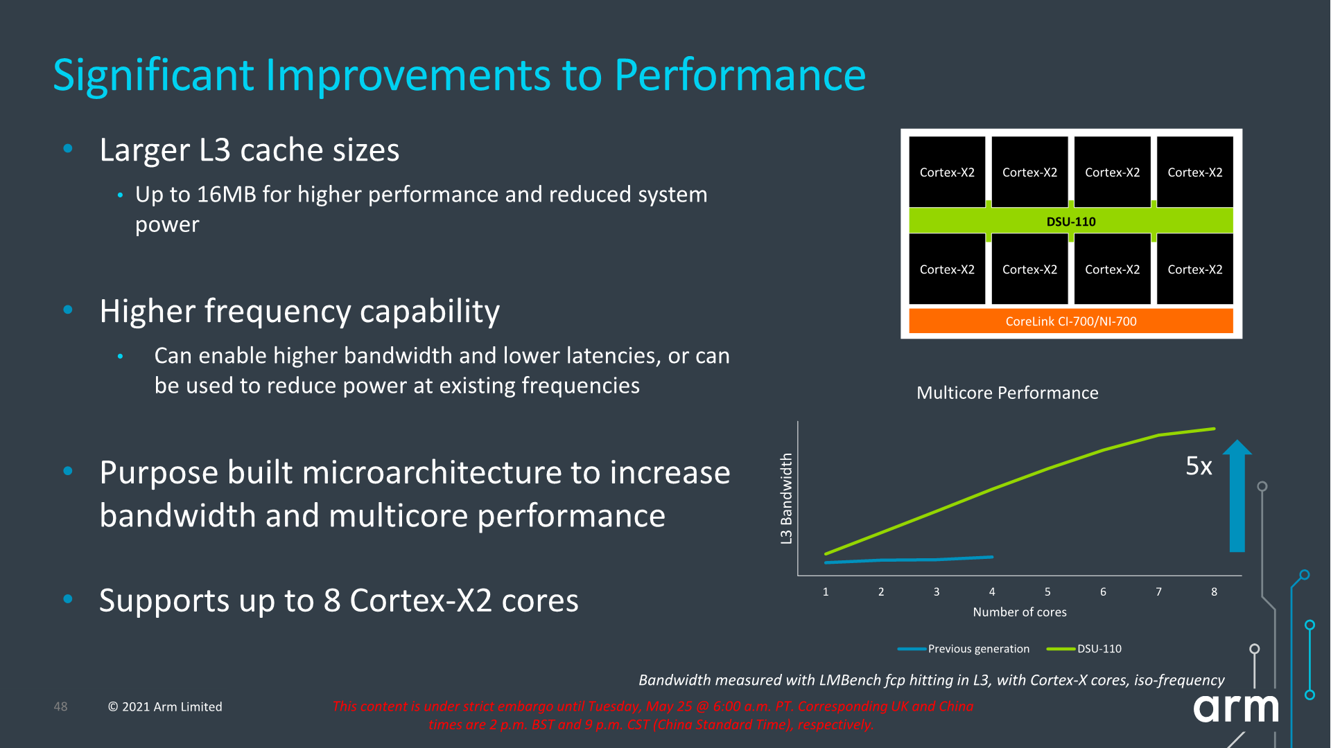
A key metric is of course the increase of L3 cache configuration which will now go up to 16MB this generation. This is of course the high-end of the spectrum and generally we shouldn’t expect such a configuration in a mobile SoC soon, but Arm has had several slides depicting larger form-factor implementations using such a larger design housing up to 8 Cortex-X2 cores. This is undoubtedly extremely interesting for a higher-performance laptop use-case.
The bandwidth increase of the new design is also significant, and applies from single-thread to multi-threaded scenarios. The new DSU-110 promises aggregate bandwidth increases of up to 5x compared to the contemporary design. More interesting is the fact that it also significantly boosts single-core bandwidth, and Arm here actually notes that the new DSU can actually support more bandwidth than what’s actually capable of the new core microarchitectures for the time being.
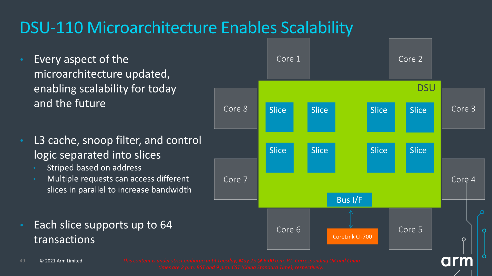
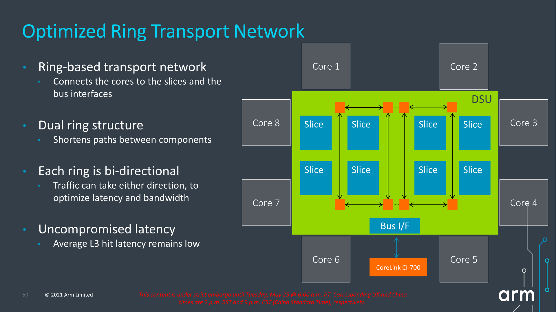
Arm never really disclosed the internal topology of the previous generation DSU, but remarks that with the DSU-110 the company has shifted over to a bi-directional dual-ring transport topology, each with four ring-stops, and now supporting up to 8 cache slices. The dual-ring structure is used to reduce the latencies and hops between ring-stops and in shorten the paths between the cache slices and cores. Arm notes that they’ve tried to retain the same lower access latencies as on the current generation DSU (cache size increases aside), so we should be seeing very similar average latencies between the two generations.
Parallel access increases for bandwidth as well as more outstanding transactions seem to have been also very important in order to improve performance, which seems very exciting for upcoming SoC designs, but also puts into more question the previously presented CPU IPC improvements and exactly how much the new DSU-110 contributes to those numbers.
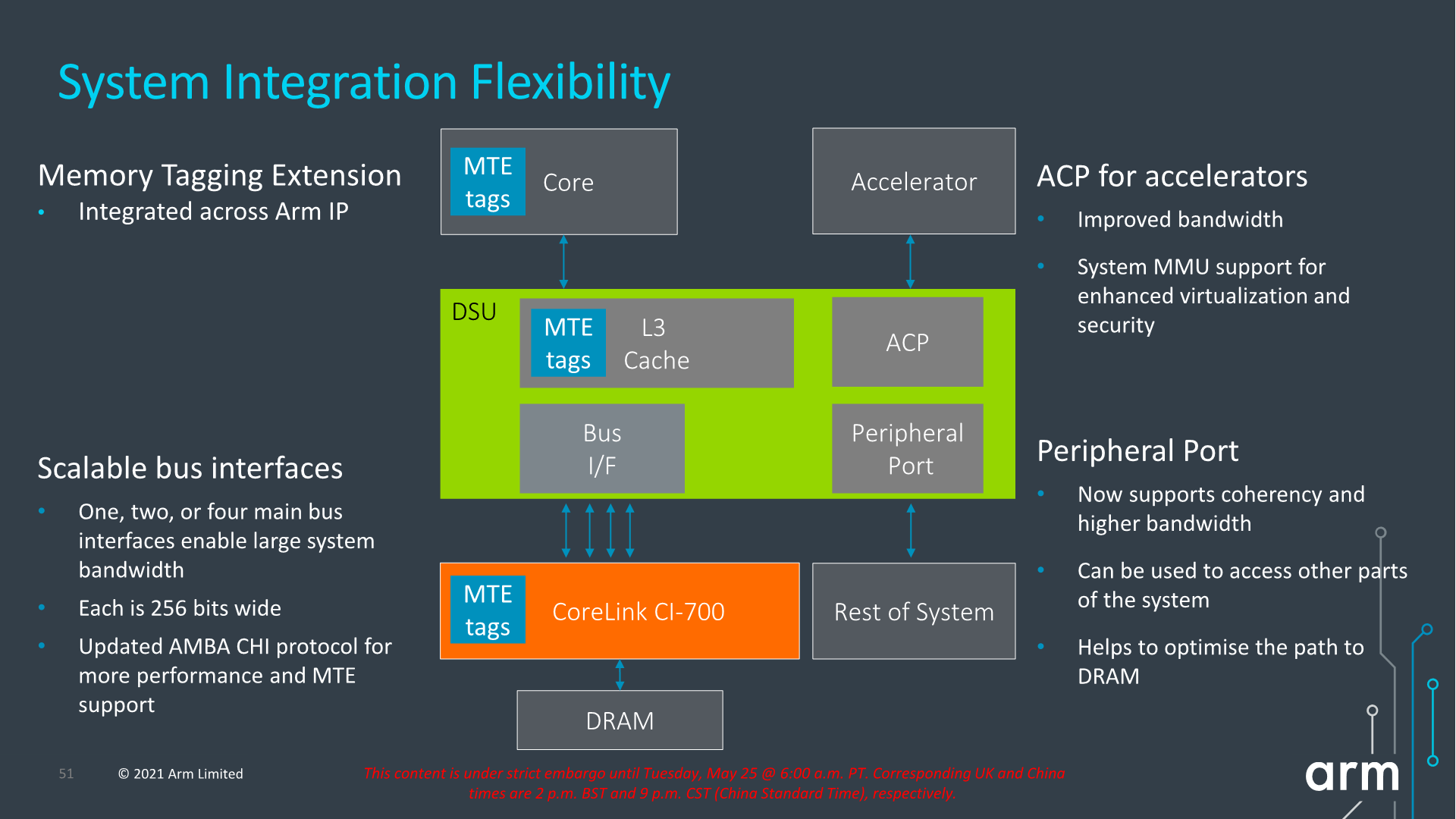
Architecturally, one important change to the capabilities of the DSU-110 is support for MTE tags, a upcoming security and debugging feature promising to greatly help with memory safety issues.
The new DSU can scale up to 4x AMBA CHI ports, meaning we’ll have up to 1024-bit total bi-directional bandwidth to the system memory. With a theoretical DSU clock of around 2GHz this would enable bandwidth of up to 256GB/s reads or writes, or double that when combined, plenty enough to be able to saturate also eventual high-end laptop configurations.

In terms of power efficiency, the new DSU offers more options for low-power operation when in idle situations, implementing partial L3 power-down, able to reduce leakage power of up to 75% compared to the current DSU.
In general idle situations but still having the full L3 powered on, the new design promises up to 25% reduction in leakage power all whilst offering 2x the bandwidth capabilities.
It’s important to note that we’re talking about leakage power here- active dynamic power is expected to generally scale linearly with the bandwidth increase of the new design, meaning 5x the bandwidth would also cost 5x the power. This would be an important factor to note into system power and in general the expected power behaviour of the next-gen SoCs when they’re put under heavy memory workloads.
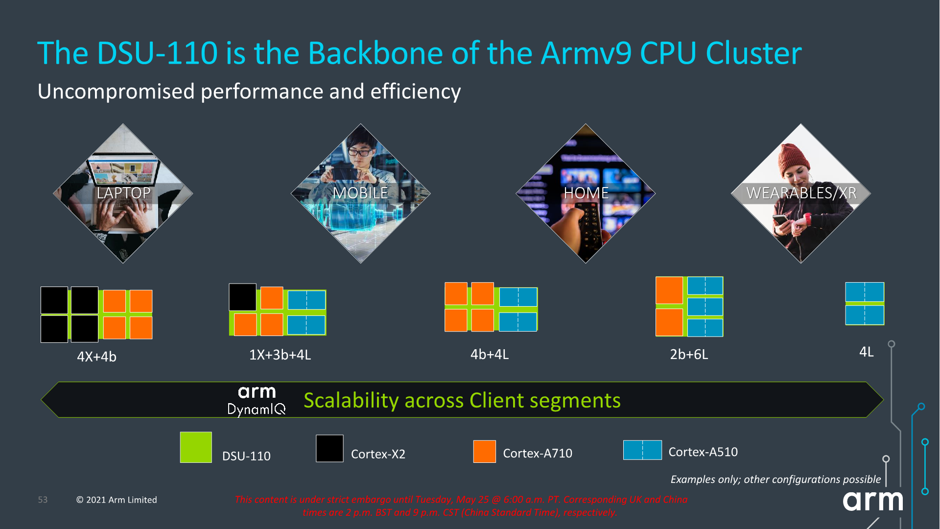
Arm describes the DSU-110 as the backbone of the Armv9 cluster and that seemingly seems to be an apt description. The new bandwidth capabilities are sure to help out both with single-threaded, but also with multi-threaded performance of upcoming SoCs. Generally, the new 16MB L3 capability, while it’s possible somebody might do a high-end laptop SoC configuration, isn’t as exciting as the now finally expected move to a new 8MB L3 on mobile SoCs, hopefully also enabling higher power efficiency and more battery life for devices.


181 Comments
View All Comments
mode_13h - Tuesday, June 1, 2021 - link
> some CPUs did mark the instruction boundaries in the cache.Not surprising, other than how far back you say it went.
mode_13h - Wednesday, May 26, 2021 - link
All good points. People who think "ISA doesn't matter" don't really understand everything an ISA encompasses.GeoffreyA - Wednesday, May 26, 2021 - link
The difference that divides them is that CISC can include a memory operation as part of an arithmetic one, whereas in RISC the two are separate (at least, in a load-store architecture).mode_13h - Wednesday, May 26, 2021 - link
> The difference that divides them is that CISC can include a memory operationI'm not an expert on the subject, but there are other elements in RISC orthodoxy, concerning things like:
* number of operands (also number of src & dst operands)
* encoding of immediates
* side-effects
I view the whole subject of CISC vs. RISC as something like MMA (Mixed Martial Arts). It turns out that there's no single best classical martial arts style. The most effective fighters use a blend of techniques adopted from various, disparate fighting styles.
GeoffreyA - Thursday, May 27, 2021 - link
"The most effective fighters use a blend of techniques"Absolutely. It's almost a universal principle that the winning design puts together the best elements from competing designs and throws away the junk.
Thala - Tuesday, May 25, 2021 - link
It does not matter that they are RISC-like inside, the issue with x86 is that they still carry the typical CISC baggage - and no internal RISC-like structure will help them here.km1810vm4 - Wednesday, May 26, 2021 - link
I would say x86 baggage. There were much nicer CISC architectures around at the time, like the Motorola 68000.TheinsanegamerN - Wednesday, May 26, 2021 - link
Intel's p5 processors implemented RISC style micro ops into their x86 decoding, that's part of why they were so dramatically faster then 486. It's not like this is hard to find out....mode_13h - Thursday, May 27, 2021 - link
> Intel's p5 processors implemented RISC style micro ops into their x86 decodingIn fact, early CPUs used a lot of microcode, and one of the ways they got faster was by replacing microcoded operations with hardwired logic. This was enabled by ever-increasing transistor budgets.
> that's part of why they were so dramatically faster then 486.
This feels like a bit of revisionist history. Here are some of the reasons why Pentium was faster than 80486:
https://en.wikipedia.org/wiki/P5_(microarchitectur...
Kamen Rider Blade - Tuesday, May 25, 2021 - link
Android needs to get their developers to stop using Java and use C/C++/Rust for their apps to eek out the max performance possible.Apple's App code base is generally C/C++, that's why they have the performance that they have.
And it's a long time nagging issue that I wish the Android community would solve.
It would give Android a HUGE performance boost to move their Apps over to C/C++/Rust.
Programming Languages have already been benchmarked against each other to see which one's faster and sorry to say it, but the C/C++/Rust family win the day in terms of Code Speed while using the same hardware platform.
https://benchmarksgame-team.pages.debian.net/bench...