Intel Core i7-11700K Review: Blasting Off with Rocket Lake
by Dr. Ian Cutress on March 5, 2021 4:30 PM EST- Posted in
- CPUs
- Intel
- 14nm
- Xe-LP
- Rocket Lake
- Cypress Cove
- i7-11700K
CPU Tests: Microbenchmarks
Core-to-Core Latency
As the core count of modern CPUs is growing, we are reaching a time when the time to access each core from a different core is no longer a constant. Even before the advent of heterogeneous SoC designs, processors built on large rings or meshes can have different latencies to access the nearest core compared to the furthest core. This rings true especially in multi-socket server environments.
But modern CPUs, even desktop and consumer CPUs, can have variable access latency to get to another core. For example, in the first generation Threadripper CPUs, we had four chips on the package, each with 8 threads, and each with a different core-to-core latency depending on if it was on-die or off-die. This gets more complex with products like Lakefield, which has two different communication buses depending on which core is talking to which.
If you are a regular reader of AnandTech’s CPU reviews, you will recognize our Core-to-Core latency test. It’s a great way to show exactly how groups of cores are laid out on the silicon. This is a custom in-house test built by Andrei, and we know there are competing tests out there, but we feel ours is the most accurate to how quick an access between two cores can happen.
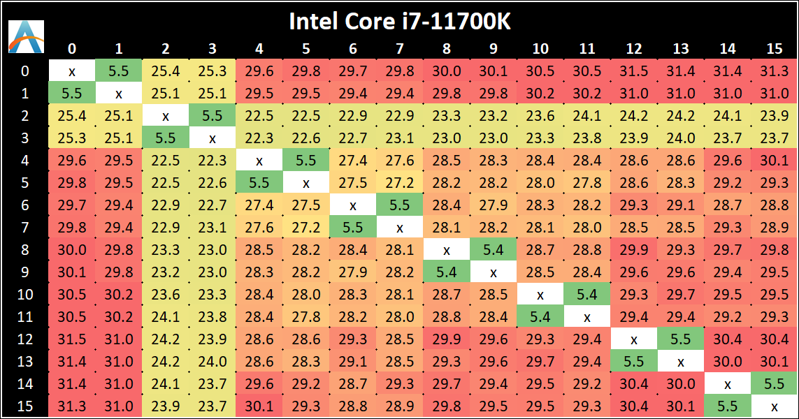
The core-to-core numbers are interesting, being worse (higher) than the previous generation across the board. Here we are seeing, mostly, 28-30 nanoseconds, compared to 18-24 nanoseconds with the 10700K. This is part of the L3 latency regression, as shown in our next tests.
One pair of threads here are very fast to access all cores, some 5 ns faster than any others, which again makes the layout more puzzling.
Update 1: With microcode 0x34, we saw no update to the core-to-core latencies.
Cache-to-DRAM Latency
This is another in-house test built by Andrei, which showcases the access latency at all the points in the cache hierarchy for a single core. We start at 2 KiB, and probe the latency all the way through to 256 MB, which for most CPUs sits inside the DRAM (before you start saying 64-core TR has 256 MB of L3, it’s only 16 MB per core, so at 20 MB you are in DRAM).
Part of this test helps us understand the range of latencies for accessing a given level of cache, but also the transition between the cache levels gives insight into how different parts of the cache microarchitecture work, such as TLBs. As CPU microarchitects look at interesting and novel ways to design caches upon caches inside caches, this basic test proves to be very valuable.
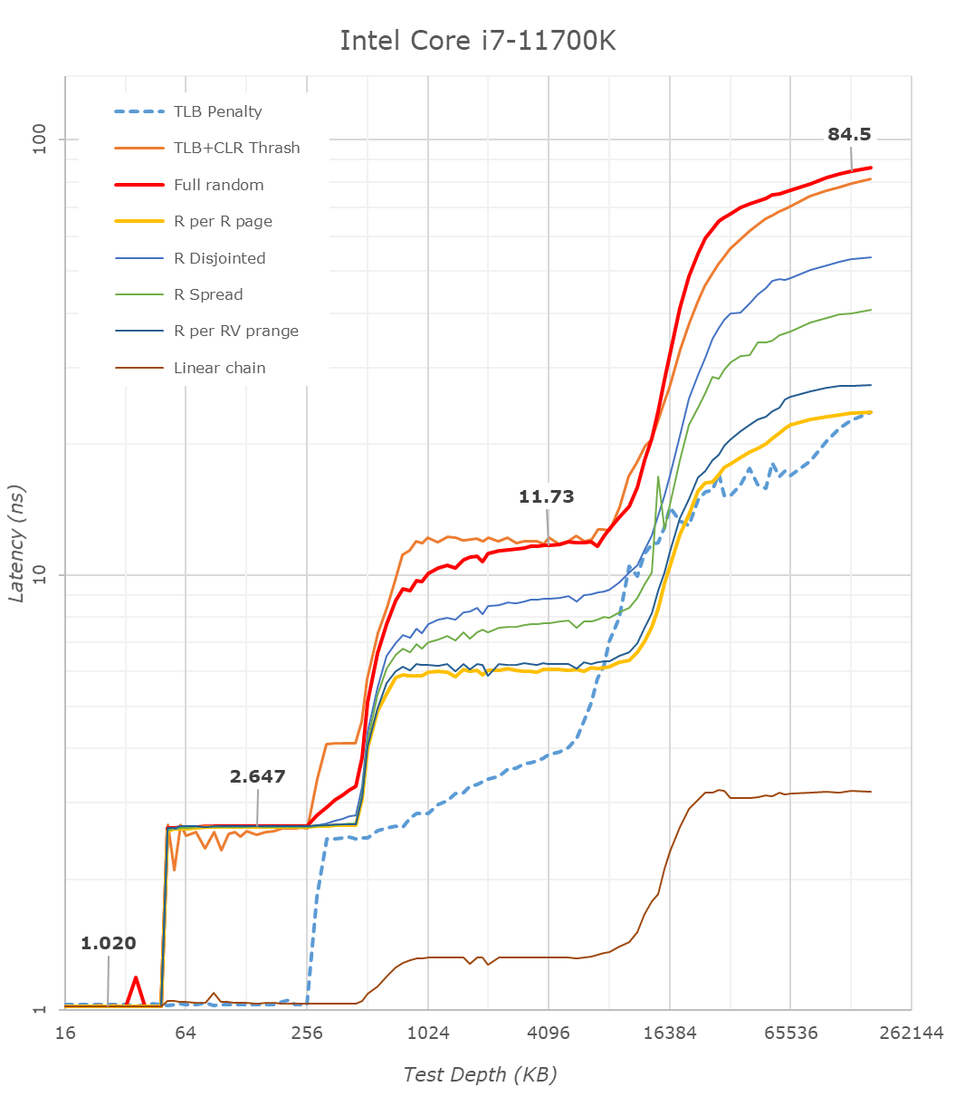
Looking at the rough graph of the 11700K and the general boundaries of the cache hierarchies, we again see the changes of the microarchitecture that had first debuted in Intel’s Sunny Cove cores, such as the move from an L1D cache from 32KB to 48KB, as well as the doubling of the L2 cache from 256KB to 512KB.
The L3 cache on these parts look to be unchanged from a capacity perspective, featuring the same 16MB which is shared amongst the 8 cores of the chip.
On the DRAM side of things, we’re not seeing much change, albeit there is a small 2.1ns generational regression at the full random 128MB measurement point. We’re using identical RAM sticks at the same timings between the measurements here.
It’s to be noted that these slight regressions are also found across the cache hierarchies, with the new CPU, although it’s clocked slightly higher here, shows worse absolute latency than its predecessor, it’s also to be noted that AMD’s newest Zen3 based designs showcase also lower latency across the board.
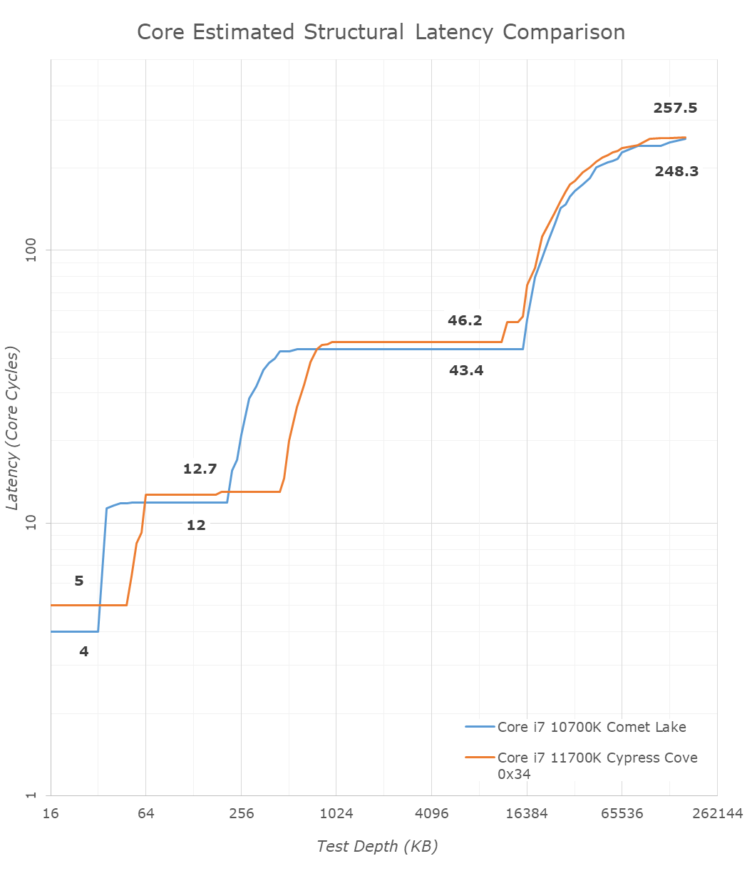
With the new graph of the Core i7-11700K with microcode 0x34, the same cache structures are observed, however we are seeing better performance with L3.
The L1 cache structure is the same, and the L2 is of a similar latency. In our previous test, the L3 latency was 50.9 cycles, but with the new microcode is now at 45.1 cycles, and is now more in line with the L3 cache on Comet Lake.
Out at DRAM, our 128 MB point reduced from 82.4 nanoseconds to 72.8 nanoseconds, which is a 12% reduction, but not the +40% reduction that other media outlets are reporting as we feel our tools are more accurate. Similarly, for DRAM bandwidth, we are seeing a +12% memory bandwidth increase between 0x2C and 0x34, not the +50% bandwidth others are claiming. (BIOS 0x1B however, was significantly lower than this, resulting in a +50% bandwidth increase from 0x1B to 0x34.)
In the previous edition of our article, we questioned the previous L3 cycle being a larger than estimated regression. With the updated microcode, the smaller difference is still a regression, but more in line with our expectations. We are waiting to hear back from Intel what differences in the microcode encouraged this change.
Frequency Ramping
Both AMD and Intel over the past few years have introduced features to their processors that speed up the time from when a CPU moves from idle into a high powered state. The effect of this means that users can get peak performance quicker, but the biggest knock-on effect for this is with battery life in mobile devices, especially if a system can turbo up quick and turbo down quick, ensuring that it stays in the lowest and most efficient power state for as long as possible.
Intel’s technology is called SpeedShift, although SpeedShift was not enabled until Skylake.
One of the issues though with this technology is that sometimes the adjustments in frequency can be so fast, software cannot detect them. If the frequency is changing on the order of microseconds, but your software is only probing frequency in milliseconds (or seconds), then quick changes will be missed. Not only that, as an observer probing the frequency, you could be affecting the actual turbo performance. When the CPU is changing frequency, it essentially has to pause all compute while it aligns the frequency rate of the whole core.
We wrote an extensive review analysis piece on this, called ‘Reaching for Turbo: Aligning Perception with AMD’s Frequency Metrics’, due to an issue where users were not observing the peak turbo speeds for AMD’s processors.
We got around the issue by making the frequency probing the workload causing the turbo. The software is able to detect frequency adjustments on a microsecond scale, so we can see how well a system can get to those boost frequencies. Our Frequency Ramp tool has already been in use in a number of reviews.
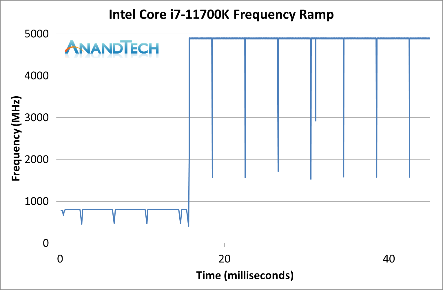
Our ramp test shows a jump straight from 800 MHz up to 4900 MHz in around 17 milliseconds, or a frame at 60 Hz.


541 Comments
View All Comments
blppt - Saturday, March 13, 2021 - link
Not really---the Bulldozer design had far more problems than just the inadequate Windows scheduler---while "optimized" linux kernels gave better performance, the true issue with Bulldozer was that you had 8 relatively weak cores versus 4 strong cores from Intel, and at the time, coders were still struggling to optimize for anything over 2 cores.In a sense, the designers of Bulldozer REALLY misread the timeline of highly multithreaded coding taking over the market. Heck, even if it was released now alongside the equivalent Core 2 quads, it would still stink for the majority of users, because no game gets any significant advantage of 4+ physical cores even today---and most games still value high single thread/core performance.
Oxford Guy - Sunday, March 28, 2021 - link
'the true issue with Bulldozer was that you had 8 relatively weak cores versus 4 strong cores from Intel, and at the time, coders were still struggling to optimize for anything over 2 cores. In a sense, the designers of Bulldozer REALLY misread the timeline of highly multithreaded coding taking over the market.'My guess is that AMD designed Bulldozer for the enterprise market and didn't want to invest in an additional design more suited to the consumer desktop space. Instead, its additional design priority was the console scam (Jaguar). While that was a good move for AMD it wasn't beneficial for consumers, as consoles are a parasitic redundancy.
One thing many ignore is that Piledriver supercomputers occupied quite high spots in the world performance lists. Mostly that was due to the majority of their work being done by the GPUs, though. Even the original Bulldozer, in Opteron branding, was used in some.
The cheapness of Piledriver chips was also probably a factor in the adoption of the design for supercomputers. Turn down the voltage/wattage so that you're in the efficient part of the improved 32nm SOI node and rely almost completely on heavily threaded code when not running GPU-specific code... and voila — you have an alternative to the monopoly-priced Intel stuff.
But, on the desktop, Piledriver was a bad joke. That's because of its very poor single-thread performance mainly. Not everything can be multi-threaded and even if it is that can mean a speed regression sometimes. The slowness of the L3, the lack of enough operations caching... the design wasn't even all that optimized for multi-thread performance — especially FPU stuff. The cores were very deeply pipelined, designed to use very high clocks. They were not efficient with avoiding bubbles and such. I read that AMD relied too heavily on automated tools due to cost sensitivity.
My vague understanding of the design is that it was narrow and deep like the Pentium 4. Why AMD tried NetBurst 2.0 is beyond me. Even for the enterprise market it's a bad move because power efficiency is important there, especially with servers (rather than supercomputers which, I think, were more tolerant of high power usage – in terms of acceptable design requirements). Even turning down the clocks/voltage to get the best efficiency from the node doesn't fix the issue of the pipelining inefficiency (although hand-tuned code used for some enterprise/scientific stuff would mask that weakness more than general-purpose consumer-grade apps would).
usiname - Monday, March 8, 2021 - link
Intel know very well that is mistake, but alder lake's big cores are not much better in term of power consumption and 10nm quality wafers so their only choice is to keep the production of max 8 core mainstream. This is bad for them, because even 3 years after AMD show 16 core mainstream they can't and as our very well known Intel they will cheat by introduce their 16 core cpu with 8 fake cores. Even more, when they introduce their "super duper" 12900k with 16 cores they will set price higher than every amd main stream and this is triple win, cheap 8 core cpu for manufacturing, better binned with higher clocks and on price of $800-1000. If you think intel trying to do something new and innovative you are wrong.GeoffreyA - Monday, March 8, 2021 - link
You may well turn out to be right about 16 cores having 8 junk ones, and knowing Intel, that's how they operate, with smoke and mirrors when they can't compete properly.Hifihedgehog - Tuesday, March 9, 2021 - link
The irony here is how Intel used to give ARM smack for having inferior single core performance while they were surpassed in multicore by the likes of Qualcomm. I believe—paraphrasing—what they would say is not all cores are created equal. Well, it looks like Intel is trying to look like they are maintaining parity when they are really just giving us mostly crappy cores that can’t perform well at all.GeoffreyA - Tuesday, March 9, 2021 - link
Also, as others have pointed out before, the nomenclature is just there to obfuscate the whole picture. Not knowing anything much about Alder Lake, I did some searching and saw that it's Golden Cove + Gracemont. Wondering what exactly GC was, I searched a little but couldn't find the answer, so I'll guess it's just Sunny Cove with a new name stuck on.Bagheera - Monday, March 8, 2021 - link
the more I read about Intel's 10nm (check relevant articles on SemiWiki and Semi accurate), the more I feel ADL is designed as a workaround for the power/thermal limitations of their 10nm process, instead of being some sort of revelation for next gen performance.Note how TGL remains Intel's only viable product on 10nm at the moment, with Ice Lake SP now two years late. I think Intel knows their 10nm may never be ready for desktop parts, so ADL is a way to have a desktop product on 10nm except not really (it's more akin to a mobile part).
It will probably do fine for gaming, but highly doubtful it will be a meaningful competition to Zen 4 for the prosumer space.
blppt - Monday, March 8, 2021 - link
Bulldozer/Piledriver were a dumb design because they relied HEAVILY on highly-threaded applications to achieve their performance. Almost none of which existed in the late 2000s when they launched. Single thread/core performance was absolutely pathetic compared to Intel's offerings at the time (Sandy Bridge and on).Zan Lynx - Sunday, March 14, 2021 - link
And yet here we are today with 8 cores in game consoles and AMD's Mantle API being the basis of both DirectX 12 and Vulkan. Multicore was always the future and it was obvious even in 2003.blppt - Monday, March 15, 2021 - link
"And yet here we are today with 8 cores in game consoles and AMD's Mantle API being the basis of both DirectX 12 and Vulkan. Multicore was always the future and it was obvious even in 200"You're missing the point. Even TODAY, few (if any) games gain an advantage of more than 4 physical cores + 4 Virtual. It is still, to this day, far more advantageous for games to have 4 strong physical cores than 8 weak ones. The latter was Bulldozer.
Never mind back in 2011/2012.