Understanding the Cell Microprocessor
by Anand Lal Shimpi on March 17, 2005 12:05 AM EST- Posted in
- CPUs
Cell’s On-Die Memory Controller
For years, we’ve known that Rambus’ memory and interface technology is well ahead of the competition. The problem is that it has never been implemented well on a PC before. The Rambus brand received a fairly negative connotation during the early days of RDRAM on the PC, and things worsened even more for the company’s brand with the Rambus vs. the DDR world lawsuits.Rambus has had success in a lot of consumer electronics devices, such as HDTVs and the Playstation 2, so when Cell was announced to make heavy use of Rambus technologies, it wasn’t too surprising. As we’ve reported before, Rambus technology is used in about 90% of the signaling pins on Cell. The remaining 10% are mostly test pins, so basically, Rambus handles all data going in and out of the Cell processor. They do so in two ways:
First off, Cell includes an on-die dual channel XDR memory controller, each channel being 36-bits wide (32-bits with ECC). Cell’s XDR memory bus runs at 400MHz, but XDR memory transfers data at 8 times the memory bus clock - meaning that you get 3.2GHz data signaling rates. The end result is GPU-like memory bandwidth of 25.6GB/s. As we’ve mentioned in our coverage of this year’s Spring IDF, memory bandwidth requirements increase tremendously as you increase the number of processor cores - with 9 total in Cell, XDR is the perfect fit. Note that the GeForce 6800GT offers 32GB/s of memory bandwidth just to its GPU, so it would not be too surprising to see the Playstation 3’s GPU paired up with its own local memory as well as being able to share system memory and bandwidth.
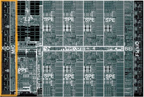
The block labeled MIC is the XDR memory controller, and the XIO block is the physical layer - all of the input receivers and output drivers are in the XIO block. Data pipelines are also present in the XIO block.
Cell’s On-Die FlexIO Interface
The other important I/O aspect of Cell is also controlled by Rambus - the FlexIO interface. Cell features two configurable FlexIO interfaces, each being 48-bits wide with 6.4GHz data signaling rates.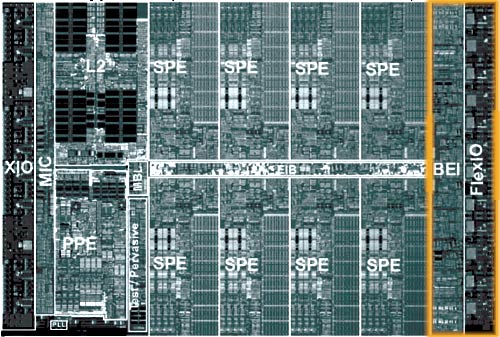
The BEI block is effectively the North Bridge interface, while the FlexIO block is the physical FlexIO layer.
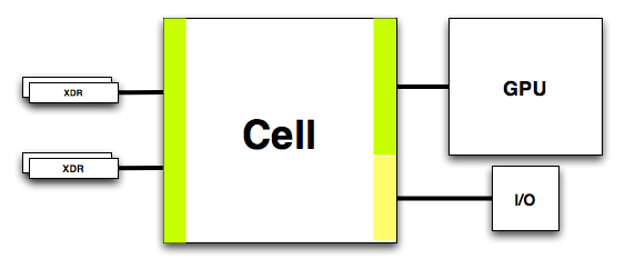
One potential implementation of Cell’s configurable FlexIO interface.
In Playstation 3, you can pretty much expect a good hunk of this bandwidth to be between NVIDIA’s GPU and the Cell processor, but it also can be used for some pretty heavy I/O interfaces.
One of the major requirements in any high performance game console is bandwidth, and thanks to Rambus, Cell has plenty of it.


70 Comments
View All Comments
faboloso112 - Thursday, March 17, 2005 - link
ahh i love bedtime stories!great read...VERY informative!
ksherman - Thursday, March 17, 2005 - link
sweet article! way over my head, but there were some parts that were dropped down to my level of understanding. Leave it to anand to tell the real story. It will be interesting to see how willing some companies will be to accomidate Sony's ratical processor... bu tas long as theirs money... Do you think that it is possible to (down the road) flop a x86 chip in place of the PPE? wouldn't hat make the Cell compatible with the current processing standards?ProviaFan - Thursday, March 17, 2005 - link
Describing this as a "sit down read" type of article makes me want to print it out to put it in the magazine rack, because I don't have a laptop + 802.11g to peruse AnandTech while I'm, er... ;)xsilver - Thursday, March 17, 2005 - link
nice, definitley one of those "sit down reads".... some serious shiznit ;)cosmotic - Thursday, March 17, 2005 - link
OMG! FIRST POST LOL ROFL LMAO OMG!!! LOOK WHOS COOL!!!Fricardo - Thursday, March 17, 2005 - link
Finally! Thanks guys.Bawl - Saturday, January 25, 2014 - link
I just love this deep analysis of one of the most mist-understanding processor of the last decade.Too bad that after spending more than a half-of-billion dollars, SonyThoshibaIBM didn't release the presumably outstanding CellTwo.
Ferrx - Sunday, December 20, 2015 - link
Hi, can you help me to understand this ? I don't understand at all about these._______ _________ ______
|Decode| | Execute | | Write |
----------- ---------------- -----------
| I1 | I2 | | | | | | | |
| I3 | I4 | | I1 | I2 | | | | |
| I3 | I4 | | I1 | | | | I2 | |
| | I4 | | | | | | I1 | I3 |
| I5 | I6 | | | | I4 | | I4 | |
| | I6 | | | I5 | | | I5 | |
| | | | | I6 | | | I6 | |
_______ _________ ______
In "Decode", each row has 2 columns. What do First and Second Column mean ?
same as "Write"
And in "Execute, each row has 3 columns. What do First, Second and Third column mean ?
And how is the process ? (The current table is about "In-Order Issue with Out-of-Order Completion").
I've read it many times, in the "Instruction Level Parallelism". But I still don't have any idea about it.
Ferrx - Sunday, December 20, 2015 - link
Aww... Can't do tab-'ing' 0__0