Imagination Announces A-Series GPU Architecture: "Most Important Launch in 15 Years"
by Andrei Frumusanu on December 2, 2019 8:00 PM ESTNew ISA & ALUs: An Extremely Wide Architecture
As mentioned, the ALU architecture as well as ISA of the new A-Series is fundamentally different to past Imagination GPUs, and in fact is very different from any other publicly disclosed design.
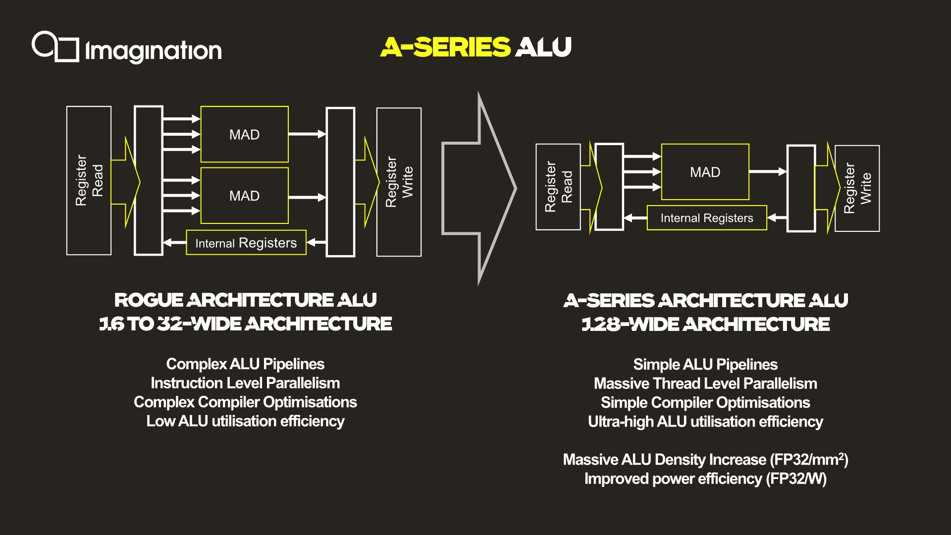
The key characteristic of the new ALU design is the fact that it’s now significantly wider than what was employed on the Rogue and Furian architectures, going to up a width of 128 execution units per cluster.
For context, the Rogue architecture used 32 thread wide wavefronts, but a single SIMD was only 16 slots wide. As a result, Rogue required two cycles to completely execute a 32-wide wavefront. This was physically widened to 32-wide SIMDs in the 8XT Furian series, executing a 32-wide wavefront in a single cycle, and was again increased to 40-wide SIMDs in the 9XTP series.
In terms of competing architectures, NVIDIA’s desktop GPUs have been 32-wide for several generations now, while AMD more recently moved from a 4x16 ALU configuration with a 64-wide wavefront to native 32-wide SIMDs and waves (with the backwards compatibility option to cluster together two ALU clusters/CUs for a 64-wide wavefront).
More relevant to Imagination’s mobile market, Arm’s recent GPU releases also have increased the width of their SIMDs, with the data paths increasing from 4 units in the G72, to 2x4 units in the G76 (8-wide wave / warp), to finally a bigger more contemporary 16-wide design with matching wavefront in the upcoming Mali-G77.
So immediately one might see Imagination’s new A-Series GPU significantly standing out from the crowd in terms of its core ALU architecture, having the widest SIMD design that we know of.
All of that said, we're a bit surprised to see Imagination use such a wide design. The problem with very wide SIMD designs is that you have to bundle together a very large number of threads in order to keep all of the hardware's execution units busy. To solve this conundrum, a key design change of the A-Series is the vast simplification of the ISA and the ALUs themselves.
Compared to the Rogue architecture as depicted in the slides, the new A-Series simplifies a execution unit from two Multiply-Add (MADD) units to only a single MADD unit. This change was actually effected in the Series-8 and Series-9 Furian architectures, however those designs still kept a secondary MUL unit alongside the MADD, which the A-Series now also does without.
The slide’s depiction of three arrows going into the MADD unit represents the three register sources for an operation, two for the multiply, and one for the addition. This is a change and an additional multiply register source compared to the Furian architecture’s MADD unit ISA.
In essence, Imagination has doubled-down on the transition from an Instruction Level Parallelism (ILP) oriented design to maximizing Thread Level Parallelism(TLP). In this respect it's quite similar to what AMD did with their GCN architecture early this decade, where they went from an ILP-heavy design to an architecture almost entirely bound by TLP.
The shift to “massive” TLP along with the much higher ALU utilization due to the simplified instructions is said to have enormously improved the density of the individual ALUs, with “massive” increases in performance/mm². Naturally, reduced area as well as elimination of redundant transistors also brings with itself an increase in power efficiency.
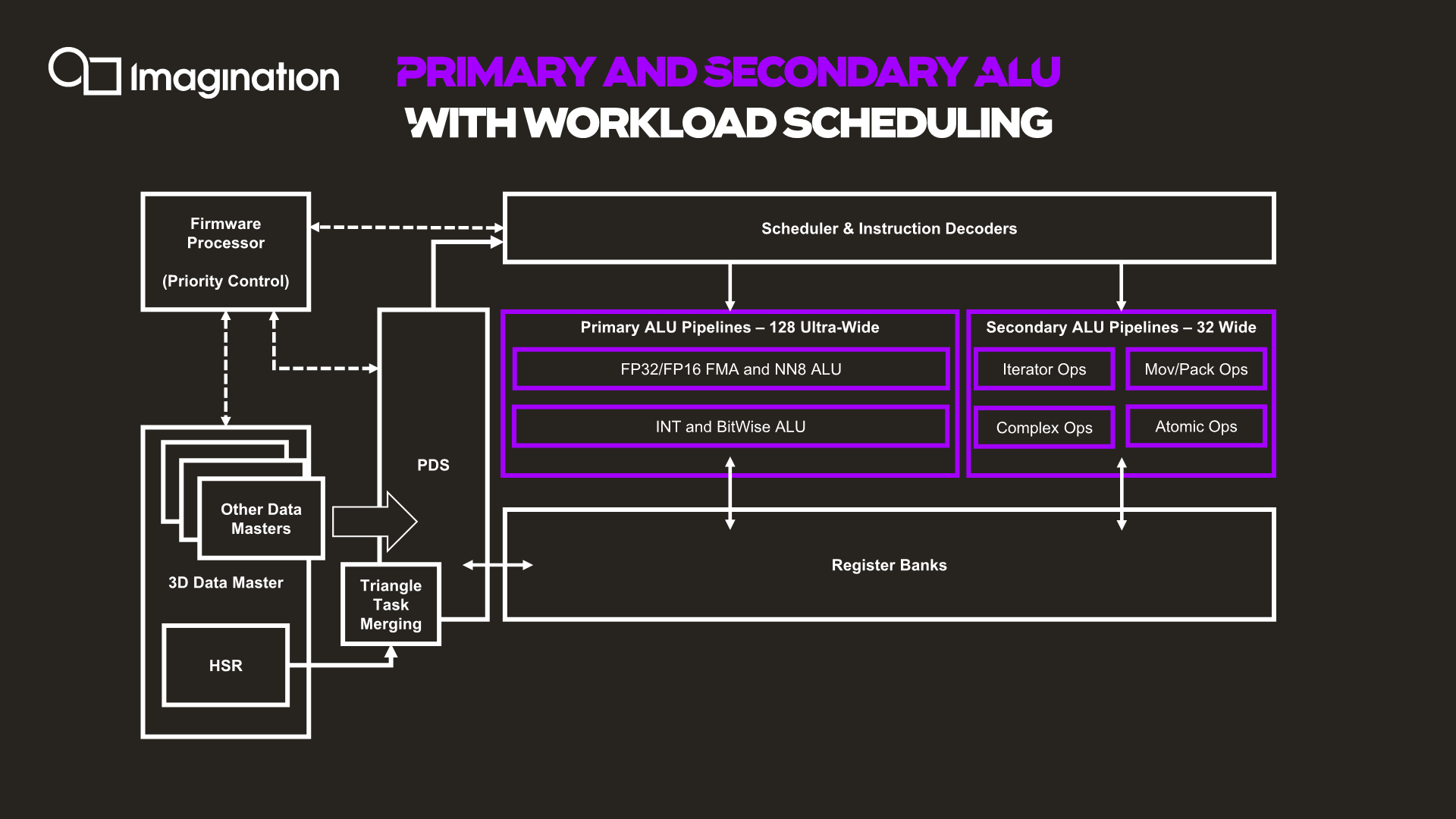
The next graphic describes the data and execution flow in the shader processor.
Things start off with a data master which kicks off work based on command queues in the memory. The 3D data master here also handles other fixed-function pre-processing, which will trigger execution of per-tile hidden surface removal and workload generation for the shader programs. The GPU here has a notion of triangle merging which groups them together into tasks in order to get better utilization of the ALUs and able to fill the 128 slots of the wavefront.
The PDS (Programmable Data Sequencer) is an allocator for resources and manager. It reserves register space for workloads and manages tasks as they’re being allocated to thread slots. The PDS is able to prefetch/preload data to local memory for upcoming threads, upon availability of the data of a thread, this becomes an active slot and is dispatched and decoded to the execution units by the instruction scheduler and decoder.
Besides the primary ALU pipeline we described earlier, there’s a secondary ALU as well. First off, a clarification on the primary ALUs is that we also find a separate execution unit for integer and bitwise operations. These units, while separate in their execution, do share the same data paths with the floating-point units, so it’s only ever possible to use one or the other. These integer units are what enable the A-Series to have high AI compute capabilities, having quad-rate INT8 throughput. In a sense, this is very similar to Arm’s NN abilities on the G76 and G77 for integer dot-product instructions, although Imagination doesn’t go into much detail on what exactly is possible.
The secondary pipeline runs at quarter rate speed, thus executing 32 threads per cycle in parallel. Here we find the more complex instructions which are more optimally executed on dedicated units, such as transcendentals, varying operations and iterators, data conversions, data moving ops as well as atomic operations.


143 Comments
View All Comments
The_Assimilator - Tuesday, December 3, 2019 - link
So what you're saying is that this "fastest GPU IP ever created" has theoretical throughput figures that are lower than a two-generation-old midrange desktop parts.Man, it's gonna be exciting when this is released and it's total unmitigated shite, like every mobile GPU ever.
ET - Wednesday, December 4, 2019 - link
For me a more useful comparison point is the consoles. Xbox One S is 1.4 TFLOPS, PS4 is 1.84 TFLOPS, and, more to the point, Switch supposedly reaches 1 TFLOPS for 16 bit at maximum, but in practice, and for 32 bit, it's around 400 GFLOPS (when docked).So in theory the AXT-64-2048 could make for quite a decent low power console chip, and a good upgrade venue for Nintendo.
(Sure, Xbox and PS have moved a little forward since then, and will move more next year, but, as an owner of a One S, I still find it quite impressive what can be achieved with this kind of GPU power.)
mode_13h - Wednesday, December 4, 2019 - link
Nintendo Switch uses the Tegra X1, which was made to be a high-end tablet SoC. So, by extension, it's not surprising that a modern candidate for that application would potentially be a worthy successor for the Switch.Speaking of set top consoles, you're citing 2013-era models (okay, the One S is more recent, but really a small tweak on the original spec). If you instead look at the PS4 Pro and One X, then you'll see that the set top consoles have moved far beyond this GPU.
Lolimaster - Tuesday, December 3, 2019 - link
The just lost it, now even qorse with amd makibg its return to arm socs.melgross - Tuesday, December 3, 2019 - link
Imagination was in trouble for a long time. The reason Apple, and Microsoft before that, left, was because Imagination refused to go along with requests from both companies for custom IP. Apple, for example needed more work on AI and ML. Imagination refused to work on that for them, which was a major mistake, as Apple was half their business, and generating more than half of their profit.When Apple announced they were developing their own GPU, they said that within two years they would no longer be using any Imagination IP. Imagination confirmed that. The assumption there was that older SoCs that Apple would continue to use for other devices would still incorporate the IP until they had been superseded by newer versions.
It’s believed that newer Apple SoCs contain no Imagination IP.
It’s interesting to see that this new Imagination IP seems to be close to what Apple wanted, but what Imagination refused to give them. A fascinating turnabout. Now it remains to be seen whether this serious improvement upon their older IP is really competitive with the newest IP from others, when it actually is in production, assuming it will really be used.
Andrei Frumusanu - Tuesday, December 3, 2019 - link
> When Apple announced they were developing their own GPU, they said that within two years they would no longer be using any Imagination IP. Imagination confirmed that.The only thing Imagination confirmed is that Apple told them that. Ironically all those press releases and all official mentions of this have disappeared from both companies, which is essentially a sign that the two companies burried the hatchets and they came under some form of agreement.
> It’s believed that newer Apple SoCs contain no Imagination IP.
Well no, we're still here two years later. Apple's GPUs still very much look like PowerVR GPUs with similar block structures, they are still using IMG's proprietary TBDR techniques, and even publicly expose proprietary features such as PVRTC. Saying Apple GPUs contain none of IMG's IP is just incompetent on the topic.
melgross - Tuesday, December 3, 2019 - link
Well, I’m going by what Apple themselves have said. So if you think they’re lying, good for you. But I’ll take their statements as fact first.Qasar - Tuesday, December 3, 2019 - link
just like you seem to do with intel ???mode_13h - Wednesday, December 4, 2019 - link
You saw that Andrei worked there 'till 2017, right? So, yeah, go ahead and argue with him. You're obviously the expert, here.Korguz - Wednesday, December 4, 2019 - link
mode_13h, of course he is. he believes all the lies and BS that intel is also saying....