Arm's New Mali-G77 & Valhall GPU Architecture: A Major Leap
by Andrei Frumusanu on May 27, 2019 12:00 AM ESTThe Mali-G77 Microarchitecture
Having covered the execution engine which is responsible for arithmetic processing, this is only part of the wider core design. Here Arm has generally kept the overall design quite similar to previous generation GPUs, however with some important changes in several blocks.
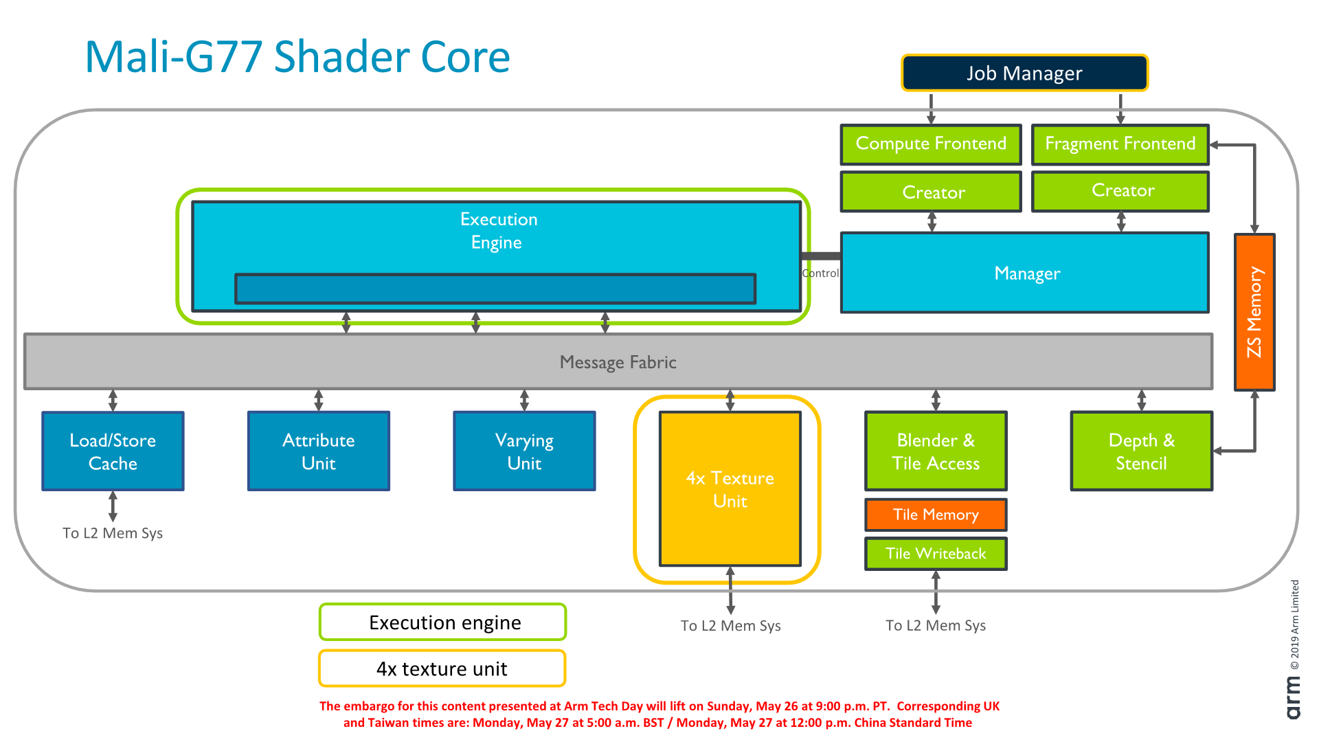
A shader core still contains the execution engine, load/store unit with cache, attribute unit, varying unit, texture mapping unit and pixel backend, as well as various other 3D fixed function blocks.
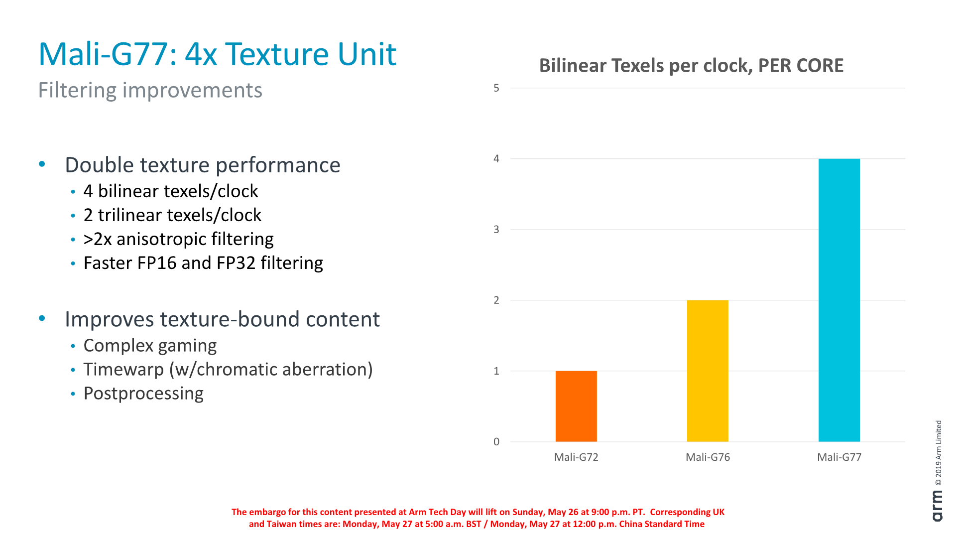
The biggest change here was on the texture unit block, which has doubled its throughput compared to the already doubled unit which we found on the Mali-G76.
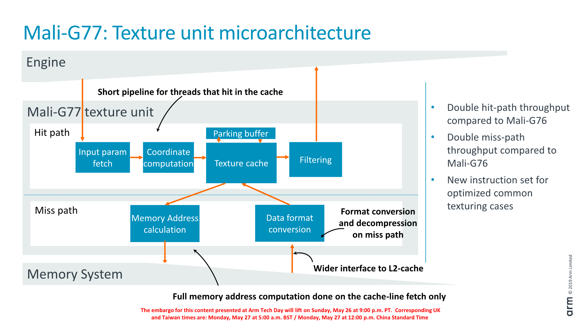
From a high-level functionality standpoint, the new TMU looks quite similar to its predecessor, however we find some very significant changes in terms of the throughput of the new design.
The design is prationioned into two “paths”, a hit- and miss-path that either deal with misses inside the cache or outside the texture cache. The hit-path is naturally a shorter more latency optimised path.
On the hit-path, the texture cache itself has been improved and is now 32KB and is able of 16 texels/cycle throughput. The filtering unit has also been improved and its throughput increased and now supports one quad per cycle for bilinear texturing, or half a quad per cycle for trilinear texturing, both 2x of G76’s throughput.
Interestingly, Arm says that the new TMU is roughly the same area as its predecessor yet still enabling this doubling of capability, which is quite a nice engineering feat.
Fundamentally this large increase in the texturing capability of a core changes the ALU:Tex ratio of the GPU. Even though ALU capability has increased by 33%, the doubling of the TMU throughput means that essentially we’re now back to a lower ratio, more in favour of texture throughput, whereas past GPUs focused on increasing the compute performance. Arm deemed this as a necessary change for workloads that are now starting to tax this aspect of GPUs more.
It’s to be noted that while the texture filtering throughput has increased, the actual pixel backend throughput has not. Here a shader core is still only able to draw out 2 pixels per clock, so we now have a 2:1 texel:pixel ratio whereas in the past it remained 1:1.
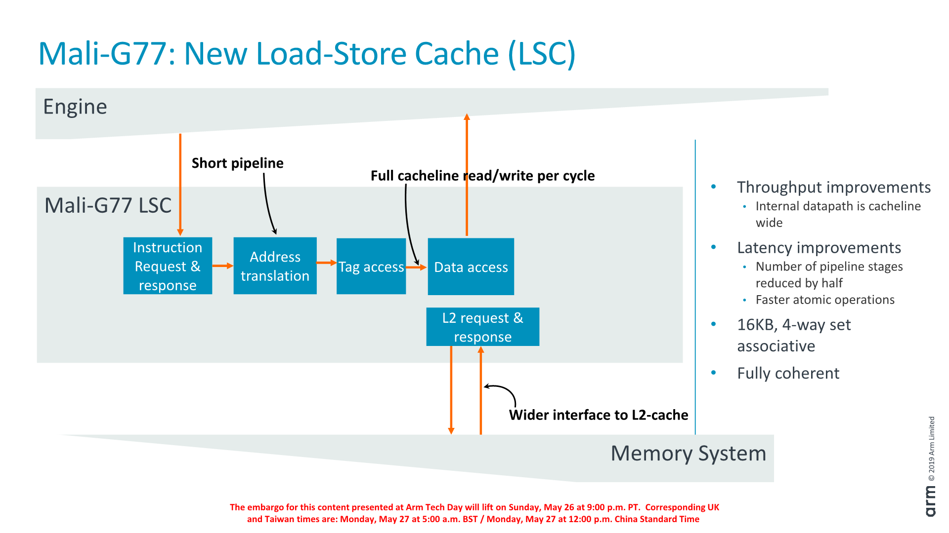
Another new redesign among the shader core blocks is a new load-store cache block. Functionally it’s the same as in the past, however it’s now been redesigned with more throughput in mind. Within the same area, the amount of pipeline stages have been reduced by half, further reducing the latency of the core’s operation. The bandwidth has been widened to a full cacheline width, which should be a doubling over its predecessor.
The actual cache is 16KB in size and 4-way set associative, and is said to be very useful for ML workloads.
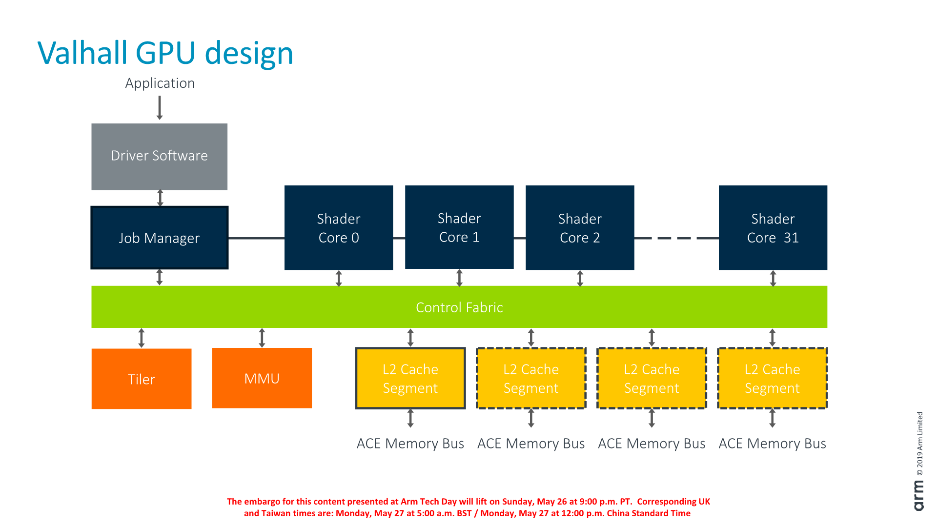
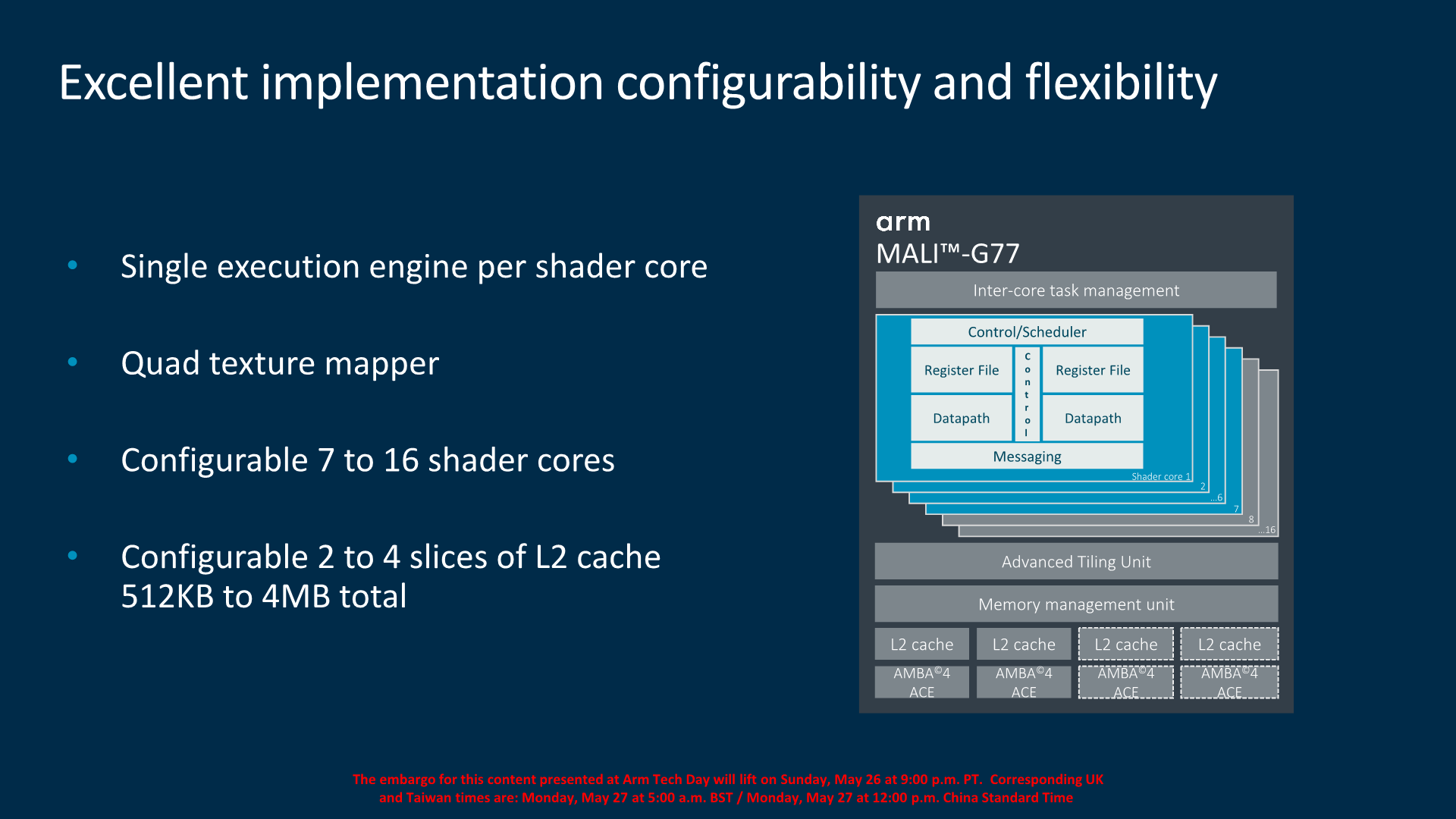
Putting all the pieces together and zooming out from a shader core to the GPU-level, we again see a large familiarity on how Arm organises its overall block. The architecture supports scaling shader cores from 1 core to 32 cores, although the microarchitecture of the G77 currently only supports up to 16 cores. Furthermore the current smallest design that Arm makes RTL ready for is a 7-core configuration, as the company deems customers going for smaller configurations would be better served by different IP (Such as the G52, or maybe a future unannounced IP in the same range).
The L2 cache still consists of up to four slices with each from 256KB to 1MB in size. Currently, most vendors have gone with 2MB configurations and I don’t think any licensee has ever implemented 4MB. In terms of bandwidth, the L2 to the LSC bandwidth has also doubled up from 32B/cycle to 64B/cycle (a full cacheline), while the external bandwidth depends on whether the vendor implements a 128-bit or 256-bit AXI interface to each of the L2 slices.


42 Comments
View All Comments
benazer - Monday, June 10, 2019 - link
Best Blogs writer good informative website.<a href="https://tasty-dinner-recipes.com/the-easy-black-fo... Dinner Recipes</a>
benazer - Monday, June 10, 2019 - link
informative website.