Upgrading from an Intel Core i7-2600K: Testing Sandy Bridge in 2019
by Ian Cutress on May 10, 2019 10:30 AM EST- Posted in
- CPUs
- Intel
- Sandy Bridge
- Overclocking
- 7700K
- Coffee Lake
- i7-2600K
- 9700K
Sandy Bridge: Outside the Core
With the growth of multi-core processors, managing how data flows between the cores and memory has been an important topic of late. We have seen a variety of different ways to move the data around a CPU, such as crossbars, rings, meshes, and in the future, completely separate central IO chips. The battle of the next decade (2020+), as mentioned previously here on AnandTech, is going to the battle of the interconnect, and how it develops moving forward.
What makes Sandy Bridge special in this instance is that it was the first consumer CPU from Intel to use a ring bus that connects all the cores, the memory, the last level cache, and the integrated graphics. This is still a similar design to the eight core Coffee Lake parts we see today.
The Ring Bus
With Nehalem/Westmere all of the cores had their own private path to the last level (L3) cache. That’s roughly 1000 wires per core, and more wires consume more power as well as being more difficult to implement the more you have. The problem with this approach is that it doesn’t work well as you scale up in things that need access to the L3 cache.
As Sandy Bridge adds a GPU and video transcoding engine on-die that share the L3 cache, rather than laying out more wires to the L3, Intel introduced a ring bus.
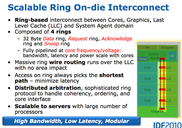
Architecturally, this is the same ring bus used in Nehalem EX and Westmere EX. Each core, each slice of L3 (LLC) cache, the on-die GPU, media engine and the system agent (fancy word for North Bridge) all have a stop on the ring bus. The bus is made up of four independent rings: a data ring, request ring, acknowledge ring and snoop ring. Each stop for each ring can accept 32-bytes of data per clock. As you increase core count and cache size, your cache bandwidth increases accordingly.
Per core you get the same amount of L3 cache bandwidth as in high end Westmere parts - 96GB/s. Aggregate bandwidth is 4x that in a quad-core system since you get a ring stop per core (384GB/s).
This means that L3 latency is significantly reduced from around 36 cycles in Westmere to 26 - 31 cycles in Sandy Bridge, with some variable cache latency as it depends on what core is accessing what slice of cache. Also unlike Westmere, the L3 cache now runs at the core clock speed - the concept of the un-core still exists but Intel calls it the “system agent” instead and it no longer includes the L3 cache. (The term ‘un-core’ is still in use today to describe interconnects.)
With the L3 cache running at the core clock you get the benefit of a much faster cache. The downside is the L3 underclocks itself in tandem with the processor cores as turbo and idle modes come into play. If the GPU needs the L3 while the CPUs are downclocked, the L3 cache won’t be running as fast as it could had it been independent, or the system has to power on the core and consume extra power.
The L3 cache is divided into slices, one associated with each core. As Sandy Bridge has a fully accessible L3 cache, each core can address the entire cache. Each slice gets its own stop and each slice has a full cache pipeline. In Westmere there was a single cache pipeline and queue that all cores forwarded requests to, but in Sandy Bridge it’s distributed per cache slice. The use of ring wire routing means that there is no big die area impact as more stops are added to the ring. Despite each of the consumers/producers on the ring get their own stop, the ring always takes the shortest path. Bus arbitration is distributed on the ring, each stop knows if there’s an empty slot on the ring one clock before.
The System Agent
For some reason Intel stopped using the term un-core in SB, and for Sandy Bridge it’s called the System Agent. (Again, un-core is now back in vogue for interconnects, IO, and memory controllers). The System Agent houses the traditional North Bridge. You get 16 PCIe 2.0 lanes that can be split into two x8s. There’s a redesigned dual-channel DDR3 memory controller that finally restores memory latency to around Lynnfield levels (Clarkdale moved the memory controller off the CPU die and onto the GPU).
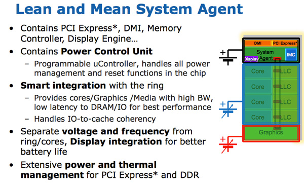
The SA also has the DMI interface, display engine and the PCU (Power Control Unit). The SA clock speed is lower than the rest of the core and it is on its own power plane.
Sandy Bridge Graphics
Another large performance improvement on Sandy Bridge vs. Westmere is in the graphics. While the CPU cores show a 10 - 30% improvement in performance, Sandy Bridge graphics performance is easily double what Intel delivered with pre-Westmere (Clarkdale/Arrandale). Despite the jump from 45nm to 32nm, SNB graphics improves through a significant increase in IPC.
The Sandy Bridge GPU is on-die built out of the same 32nm transistors as the CPU cores. The GPU is on its own power island and clock domain. The GPU can be powered down or clocked up independently of the CPU. Graphics turbo is available on both desktop and mobile parts, and you get more graphics turbo on Sandy Bridge.
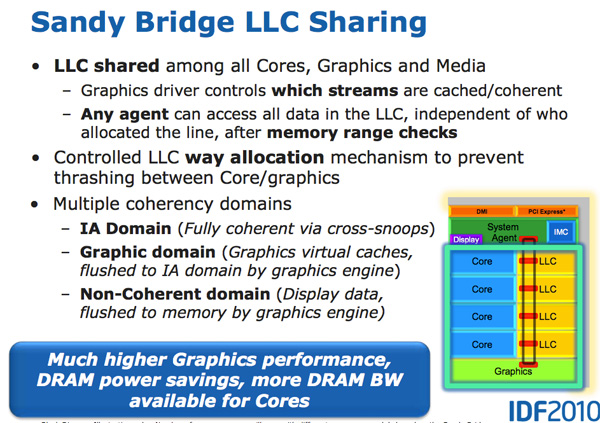
The GPU is treated like an equal citizen in the Sandy Bridge world, it gets equal access to the L3 cache. The graphics driver controls what gets into the L3 cache and you can even limit how much cache the GPU is able to use. Storing graphics data in the cache is particularly important as it saves trips to main memory which are costly from both a performance and power standpoint. Redesigning a GPU to make use of a cache isn’t a simple task.
SNB graphics (internally referred to as Gen 6 graphics) makes extensive use of fixed function hardware. The design mentality was anything that could be described by a fixed function should be implemented in fixed function hardware. The benefit is performance/power/die area efficiency, at the expense of flexibility.
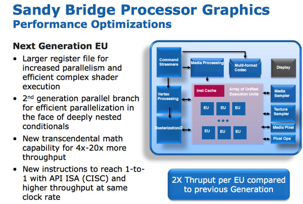
The programmable shader hardware is composed of shaders/cores/execution units that Intel calls EUs. Each EU can dual issue picking instructions from multiple threads. The internal ISA maps one-to-one with most DirectX 10 API instructions resulting in a very CISC-like architecture. Moving to one-to-one API to instruction mapping increases IPC by effectively increasing the width of the EUs.
There are other improvements within the EU. Transcendental math is handled by hardware in the EU and its performance has been sped up considerably. Intel told us that sine and cosine operations are several orders of magnitude faster now than they were in pre-Westmere graphics.
In previous Intel graphics architectures, the register file was repartitioned on the fly. If a thread needed fewer registers, the remaining registers could be allocated to another thread. While this was a great approach for saving die area, it proved to be a limiter for performance. In many cases threads couldn’t be worked on as there were no registers available for use. Intel moved from 64 to 80 registers per thread and finally to 120 for Sandy Bridge. The register count limiting thread count scenarios were alleviated.
At the time, all of these enhancements resulted in 2x the instruction throughput per EU.

Sandy Bridge vs. NVIDIA GeForce 310M Playing Starcraft 2
At launch there were two versions of Sandy Bridge graphics: one with 6 EUs and one with 12 EUs. All mobile parts (at launch) will use 12 EUs, while desktop SKUs may either use 6 or 12 depending on the model. Sandy Bridge was a step in the right direction for Intel, where integrated graphics were starting to become a requirement in anything consumer related, and Intel would slowly start to push the percentage of die area dedicated to GPU. Modern day equivalent desktop processors (2019) have 24 EUs (Gen 9.5), while future 10nm CPUs will have ~64 EUs (Gen11).
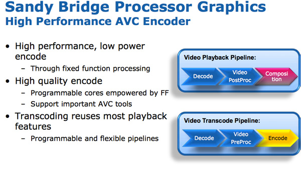
Sandy Bridge Media Engine
Sitting alongside the GPU is Sandy Bridge’s Media processor. Media processing in SNB is composed of two major components: video decode, and video encode.
The hardware accelerated decode engine is improved from the current generation: the entire video pipeline is now decoded via fixed function units. This is contrast to Intel’s pre-SNB design that uses the EU array for some video decode stages. As a result, Intel claims that SNB processor power is cut in half for HD video playback.
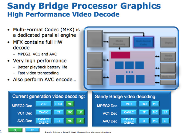
The video encode engine was a brand new addition to Sandy Bridge. Intel took a ~3 minute 1080p 30Mbps source video and transcoded it to a 640 x 360 iPhone video format. The total process took 14 seconds and completed at a rate of roughly 400 frames per second.
The fixed function encode/decode mentality is now pervasive in any graphics hardware for desktops and even smartphones. At the time, Sandy Bridge was using 3mm2 of the die for this basic encode/decode structure.
New, More Aggressive Turbo
Lynnfield was the first Intel CPU to aggressively pursue the idea of dynamically increasing the core clock of active CPU cores while powering down idle cores. The idea is that if you have a 95W TDP for a quad-core CPU, but three of those four cores are idle, then you can increase the clock speed of the one active core until you hit a turbo limit.
In all current generation processors the assumption is that the CPU reaches a turbo power limit immediately upon enabling turbo. In reality however, the CPU doesn’t heat up immediately - there’s a period of time where the CPU isn’t dissipating its full power consumption - there’s a ramp.
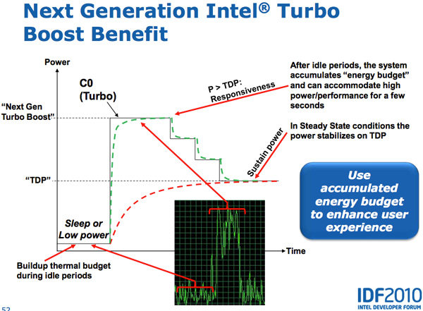
Sandy Bridge takes advantage of this by allowing the PCU to turbo up active cores above TDP for short periods of time (up to 25 seconds). The PCU keeps track of available thermal budget while idle and spends it when CPU demand goes up. The longer the CPU remains idle, the more potential it has to ramp up above TDP later on. When a workload comes around, the CPU can turbo above its TDP and step down as the processor heats up, eventually settling down at its TDP. While SNB can turbo up beyond its TDP, the PCU won’t allow the chip to exceed any reliability limits.
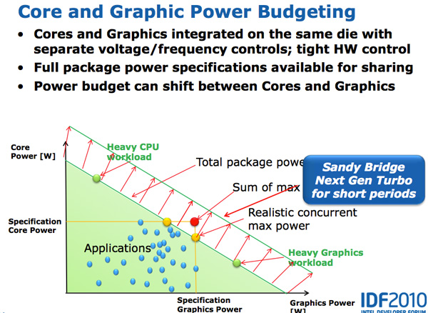
Both CPU and GPU turbo can work in tandem. Workloads that are more GPU bound running on SNB can result in the CPU cores clocking down and the GPU clocking up, while CPU bound tasks can drop the GPU frequency and increase CPU frequency. Sandy Bridge as a whole was a much more dynamic of a beast than anything that’s come before it.


213 Comments
View All Comments
Death666Angel - Sunday, May 12, 2019 - link
I've done some horrendous posts when I used my phone to make a comment somewhere. Mostly because my phone is trained to my German texting habits and not my English commenting habits. And trying to mix them leads to sub par results in both areas, so I mostly stick to using my phone for texting and my PC and laptop for commenting. But sometimes I have to write something via my phone and it makes a beautiful mess if I'm not careful.Death666Angel - Sunday, May 12, 2019 - link
Well, laptops and desktops (with monitors) are in a different category anyway, at least that's how I see it. :-)I work with a 13.3" laptop with a 1440p resolution and 150% scaling. It's not fun, but it does the job. The advantage of the larger screen real estate with a 15" or 17" laptop is outweight by the size and weight increase. I've also done work on 1024x768 monitors and it does the job in a pinch. But I've tried to upgrade as soon as the new technology was established, cheap and good enough to make it worth it without having to pay the early adopter fee or fiddle around to get it to work. Even before Win7 made it a breeze to have multiple windows in an orderly grid, I took full advantage of a multi window and multi program workflow for research, paper/presentation writing, editing and media consumption. So it is a bit surprising to see someone like Ian, a tech enthusiast with a university doctorate be so late to great tech that can really make life easier. :D
Showtime - Saturday, May 11, 2019 - link
Great article. Was hoping to see all the CPU's tested (my 4770k), but I think it shows enough. This isn't the 1st article showing that lesser CPU's can run close to the best CPU's when it come to 4k gaming. Does that look to change any time soon? I was thinking I should upgrade this year, but would like to know if I should be shooting for an 8 core, or if a 6 will be a decent enough upgrade.Consoles run slower 8 core proc's that are utilized more efficiently. At some point won't pc games do the same?
Targon - Tuesday, May 14, 2019 - link
There is always the question about what you do on your computer, but I wouldn't go less than 8 cores(since 4-core has become the base on the desktop, and even laptops should never be sold with only 2 cores IMO). If you look at the history, when AMD wasn't competitive and Intel stopped trying to actually innovate, quad-core was all you saw on the desktop, so game developers didn't see a reason to support more threads(even though it would have made sense). Once Ryzen came out with 8 cores, and Intel finally responded, you have to expect that every game developer will design with the potential that players will have 8+ core processors, so why not design with that in mind?Remember, a program that is properly multi-threaded in design will work on lower-core processors, but will scale up well when processors with more cores are being used. So going forward, quad-core would work, but 8 or more threads WILL feel a lot better, even for overall use.
CaedenV - Saturday, May 11, 2019 - link
This was a fascinating article! And what I am seeing in the real world seems to reflect this.For the most part, the IPC for general use has improved, but not by a whole lot. But if doing anything that hits the on-chip GPU, or requiring any kind of decrypt/encrypt, then the dedicated hardware in newer chips really makes a big difference.
But at the end of the day, in real-world scenarios, the CPU is simply not the bottle neck for most people. I do a lot of video ripping (all legally purchased, and only for personal use), and the bottleneck is squarely on the Blu-Ray drive. I recently upgraded from a 4x to a 10x drive, and the performance bump was exactly what was expected. Getting a faster CPU or GPU will not help there.
I do a bit of video editing, and the bottle-neck there is still almost always in storage. The 1gbps connection to the NAS, and the 1GBps connection to my RAID0 of SSDs.
I do a bit of gaming at 4k, and again the bottleneck there is squarely on the GPU (GTX1080), and as your tests show, at lower resolution my chip will be slower than a new chip... but still faster than the 60-120fps refresh of the monitor.
The real reason for an upgrade simply isn't the CPU for most people. The upgrade is the chipset. Faster/more RAM, M.2 SSDs, more available throughput for expansion cards, faster USB/USB-C ports, and soon(ish) 10gig Ethernet. These are the things that make life better for the enthusiast and the normal user; and the newer CPUs are simply more capable of taking advantage of all the extra throughput, where Sandy Bridge would perhaps choke when dealing with these newer and faster interfaces that are not available to it.
All that said; I am still not convinced to upgrade. Every previous computer was simply broken, or could not do something after 2-3 years, so an upgrade was literally necessary. But now... my computer is some 8 years old now, and I am amazed at the fact that it still does it all, and does it relatively quickly. Without it being 'broken' it is hard to justify dropping $1000+ into a new build. I mean... I want to upgrade. But I also want to do some house projects, and replace a car, and do stuff with the kids... *sigh* priorities. Part of me wishes that it would break to give me proper motivation to replace it.
webdoctors - Saturday, May 11, 2019 - link
Great timing, I've been using the same chip for 7 or 8 years now and never felt the need to upgrade until this year, but I will upgrade end of this year. DDR4 finally dropped in price and my GTX1070TI I think is getting throttled when the CPU ain't overclocked.atomicWAR - Saturday, May 11, 2019 - link
Gaming at 4K with a i7 3930K @ 4.2ghz (4.6ghz capable when needed) with 2 GTX 1080s...I was planning a new build this year but after reading this I may hold off even longer.wrkingclass_hero - Sunday, May 12, 2019 - link
I've got a 3930K as well. I was planning on upgrading to Threadripper 3 when that comes out, but if it gets delayed I may wait a bit longer for a 5mm Threadripper.mofongo7481 - Saturday, May 11, 2019 - link
I'm still using a sandy bridge i5 2400 overclocked to 3.6Ghz. Still playing modern stuff @ 1080p and pretty enjoyable.Danvelopment - Sunday, May 12, 2019 - link
I think the conclusion is slightly off for gaming, from what I could see it's not that the newer processors were only better higher resolutions, it's that the newer systems were better able to keep the GPU fed with data, resulting in a higher maximum frame rate.So at lower resolutions/quality settings, when the GPUs could let loose they could achieve much higher FPS.
My conclusion from the results wouldn't be to keep it for higher res gaming, but to keep it for gaming if you're still using a 60Hz display (which I am). I bet if you tuned quality settings for all of the GPUs to run at 60 FPS your results would sit pretty close at any resolution.
I'm currently running an E5-2670 for my gaming machine with quad channel DDR3 (4x8GB) and a 1070. That's the budget upgrade path I'd probably recommend at 60Hz.