The iPhone XS & XS Max Review: Unveiling the Silicon Secrets
by Andrei Frumusanu on October 5, 2018 8:00 AM EST- Posted in
- Mobile
- Apple
- Smartphones
- iPhone XS
- iPhone XS Max
The Apple A12 - First Commercial 7nm Silicon
Over the last few years Apple’s silicon design teams have been at the forefront of both architecture design and adopting bleeding-edge manufacturing processes. The Apple A12 is yet another generational jump for the company, as it’s able to claim to be the first commercially available piece of 7nm silicon.
When talking about process nodes, generally speaking the smaller the figure, the smaller the transistor features are. While the actual name of recent nodes have long lost any meaning in correlation to actual physical sizes, they still represent a jump in density, and thus, the ability for vendors to pack in more transistors in the same die space.
We thank TechInsights for publicly sharing their picture of the Apple A12, and we’ve followed up with posting a quick first analysis reaction to the die shot:
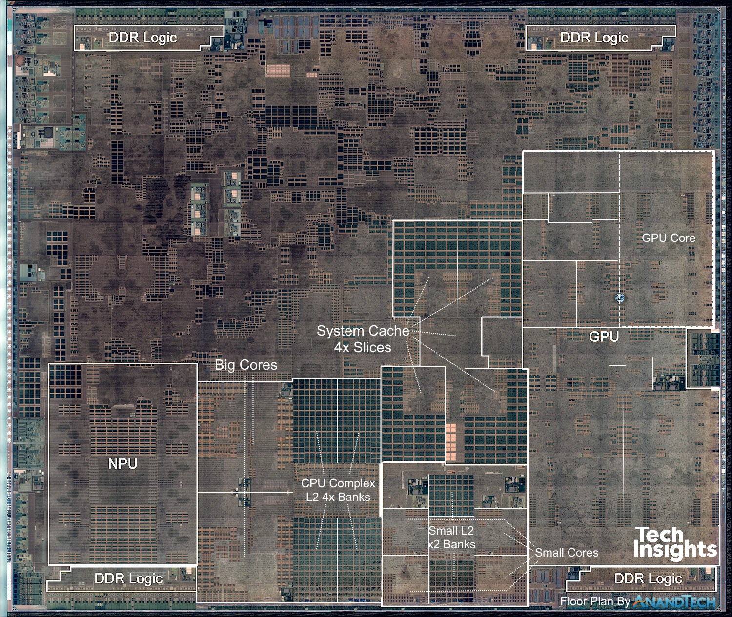
AnandTech modified TechInsights Apple A12 Die Shot
Going over it again here for this article, I’ve put down my own custom labelling and interpretation of the die shot. The new A12 largely follows Apple’s SoC layout structure (90° rotated to most past die shots).
On the right side we see the GPU complex with the four GPU cores and shared logic in the middle. The CPU complex is found at the bottom, with the two Vortex big CPU cores on the centre-left, divided by the big L2 cache, right next to the four small Tempest CPU cores and their own L2 cache.
The four big chunks of SRAM in the middle blocks are part of the system cache – this is a SoC-wide cache layer in between the memory controllers and the internal system interconnect & block memory subsystems. Here Apple uses this block as an energy saving feature: Because memory transactions to DRAM are quite expensive in terms of energy usage, being able to cache things on-chip will save a great amount of power, with the added benefit of possible performance increases due to the locality of the data.
The Apple A12’s system cache has, to date, seen the biggest change since its introduction in the Apple A7. The big change in layout also points out to a large change in the functionality of the block, as now we clearly see a separation of the block into what’s apparent to be four slices. On previous Apple SoCs such as in the A11 or A10, the system cache looked more like a single block of logic, with what appeared to be two slices. A doubling of the slices could possibly point out to a very large change in the memory performance of this block – something I very much believe to be the case following more analysis in the coming pages.
Finally, the last big introduction in the A12 is a major revamp of the neural accelerator IP. Here Apple claims to have moved from a dual-core design found in the A11, to a new 8-core design. Last year’s design was rumoured to be a CEVA IP – although we’ve never have full confirmation on that as Apple doesn’t want it to be known.
During the keynote presentation it’s important to note that Apple never mentioned that this is an in-house design, something the marketing materials was always eager to point out for other IP blocks of the SoCs.
Edit: I've been notified that Apple does have the "Apple-designed" mention on the A12 webpage, meaning this does indeed mean it's an in-house IP.
The A12 being an 8-core design would point out to a 4x increase in performance – but the actual increase is near 8x, increasing from 600GigaOPs in the A11 to 5TeraOPs in the A12. In the die shot we see the 8 MAC engines surrounding a big central cache, with possible shared logic at the top that would be responsible for fixed function and fully connected layer processing.
| Die Block Comparison (mm²) | ||
| SoC Process Node |
Apple A12 TSMC N7 |
Apple A11 TSMC 10FF |
| Total Die | 83.27 | 87.66 |
| Big Core | 2.07 | 2.68 |
| Small Core | 0.43 | 0.53 |
| CPU Complex (incl. cores) | 11.90 | 14.48 |
| GPU Total | 14.88 | 15.28 |
| GPU Core | 3.23 | 4.43 |
| NPU | 5.79 | 1.83 |
Looking over the different block size changes from the A11 to the A12, we see the benefits of TSMC’s newer 7nm manufacturing node. It’s to be noted that nearly all IP blocks have undergone changes, so it’s not really a valid apples-to-apples comparison to determine just how much density has improved with the new manufacturing node. Still, taking a single GPU core as a possible candidate (as we largely see the same structure), we see a 37% decrease in size compared to the A11. It’s quite obvious that the new node has enabled Apple to add an additional GPU core even though in absolute terms, the GPU is still smaller in the A12.
A bigger CPU and a massive cache hierarchy
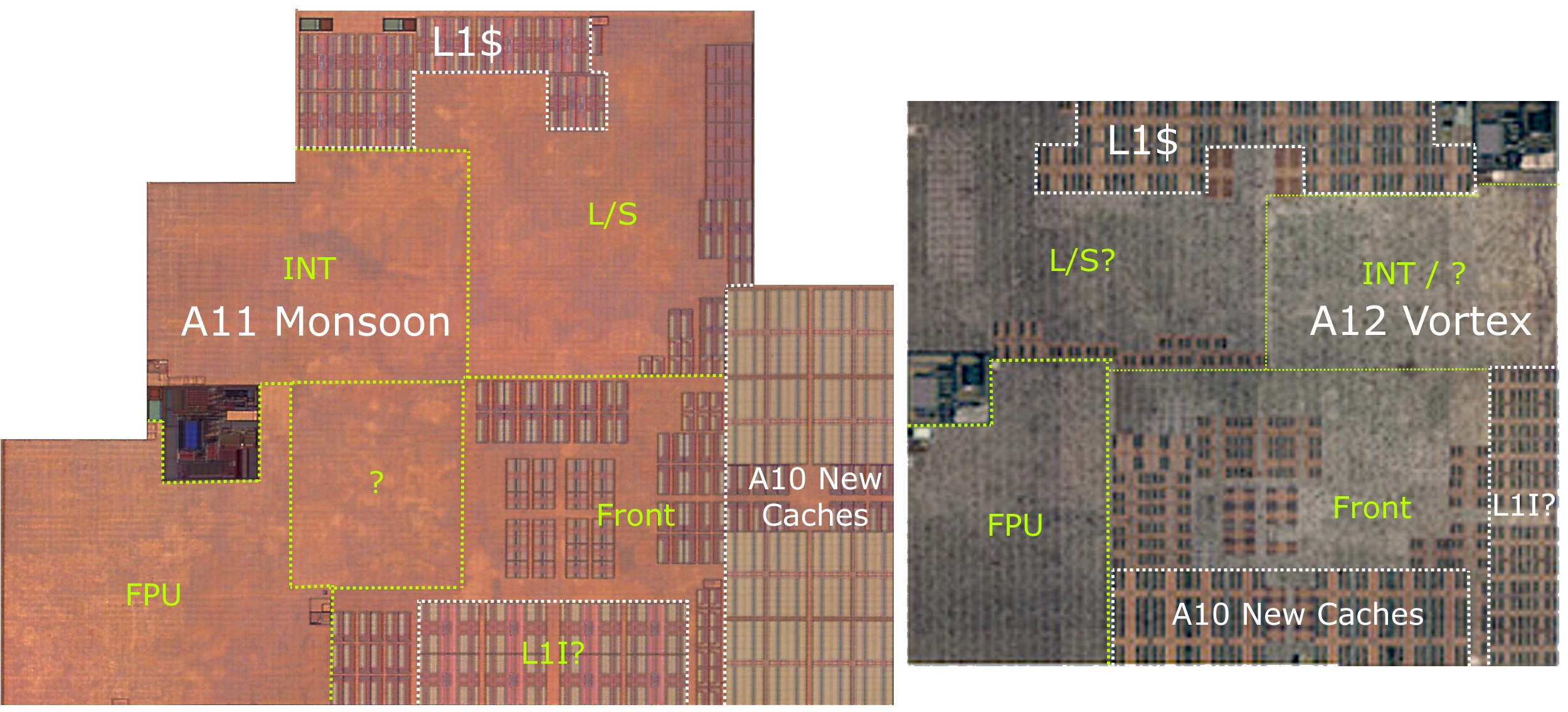
Credit: TechInsights Apple A12 Die Shot, ChipRebel Apple A11 Die Shot
Moving on to the CPU complex, and in particular the new big CPU core, we now see what is possibly Apple’s biggest change in its CPU layout in several generations. In particular, we see a doubling of the L1 data caches in the new Vortex CPU, increasing from 64KB to 128KB in the new core. In the front-end, we also saw a doubling of the SRAM blocks that I attribute to the L1 instruction caches – which I now believe to have also seen doubling to 128KB. It’s funny that even after several years, we still haven’t really figured out what the A10 had introduced into the front-end block: here we saw a new very large block of cache whose function largely remains unclear.
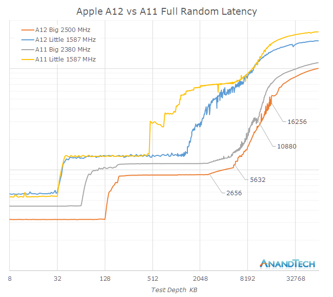
A big question over the years has been what Apple’s cache hierarchy actually looks like. Looking at the memory latency behaviour at different test depths, we see the different jumps at different test depths. I didn’t annotate the latency values as we’ll revisit them later in a non-logarithmic version of this graph.
On the big core side, we clearly see the L1$ jump from 64KB to 128KB, and I think there’s no doubt about the increases here. Moving into the L2 cache however, we’re seeing some odd behaviour in terms of the latency. It’s clear that around the 3MB range that there’s an increasing jump in latency, up until around 6MB. It’s to be noted that this behaviour of a slower second 3MB only happens when accessing in a fully random patterns, in smaller access windows the latency is flat up until 6MB.
Not dwelling more into this for now, we move into the area beyond 6MB that is served by the system cache. It’s hard to make it out at first because there’s an offset caused by overall lower latency, but in general the latency curve goes around 4MB further before we reach mostly DRAM latencies. This corresponds to what we actually see on the die: the new system cache not only has seen a doubling of its slices, but has also outright doubled in capacity from 4 to 8MB.
Moving onto an analysis of the little cores, things become a bit more complex. At first glance you would believe the A11’s small cores L2 was limited to 512KB and that the A12 goes up to 1.5MB, however what I think is going on is that we’re being tricked by the power management policy of the cache. Looking at the A11 Mistral core latency, we see some obvious jumps at 768KB and 1MB. A similar jump can be seen in the A12 cores at 2MB.
It’s at this point, where it’s best to go back to the die shots and do some pixel counting, and we come up with the following table:
| Measured and Estimated Cache Sizes | ||
| SoC | Apple A12 | Apple A11 |
| Big L1$ | 128KB | 64KB |
| Big L2$ | 128 instances 6MB per core/thread 8MB total at 64KB/inst |
128 instances 6MB per core/thread 8MB total at 64KB/inst |
| Small L1$ | 32KB | 32KB |
| Small L2$ | 32 instances 1.5MB per core/thread 2MB total at 64KB/inst |
16 + 2(?) instances 512KB per core/thread 1MB total at 64KB/inst |
| System Cache | 4x 16 instances (double size) 8MB at 128KB/inst |
2x 32 instances 4MB at 64KB/inst |
The big core L2’s haven’t seen any structural changes between the A11 and A12 – both have 128 instances of SRAM macros, separated into two chunks. The question here remains that if the L2 is indeed just 6MB, then that would mean 48KB per SRAM block.
When looking at the small cores, we see that they use identical SRAM macros. The A12’s small core L2 has doubled from 16 to 32 instances, meaning there must have been a doubling. However as we see that the measured latency depth of the L2 has at least tripled, something else must be going on. What we’re measuring by no means has to represent what’s in the hardware, and indeed we can confirm this by running the latency test in a more special manner that makes the power management think it’s just some minor workload. On the A12, the Tempest cores then appear to have only 512KB available to them.
The conclusion is here is that Apple is employing partial cache power-down in what seems to be per-bank granularity. On the A12 each small core L2 bank is 512KB, and on the A11 it’s 256KB. Also, this more strongly leads me to believe there’s 2MB on the A12 and 1MB on the A11, it’s just that the test probably doesn’t fulfill the policy requirements to access the full cache.
In turn, because this would confirm 64KB per SRAM instance, we can go back and make some hypotheses about the big core L2’s. Again, looking at it, one would believe it stops at 6MB, but looking closer, especially on the A12, there is a change of behaviour at 8MB. Again it’s likely that the cores have 8MB of physical cache, and there’s an obvious change in access behaviour once we’re nearing a full cache.
The take-away here is that Apple’s caches are just immense, and the A12 further expands in that regard by doubling the system cache size. In practice, we have around 16MB of useable cache hierarchy on the part of the big CPU cores – a massive amount that just puts the memory and cache subsystems of competing SoCs to shame.
An evolutionary GPU
On the GPU side of things, we had some big expectations from the A12, not merely in terms of performance, but also in terms of architecture. Last year there had been a press release from Imagination stating that Apple had informed them that the company planned to no longer use its IP in new products in 15 to 24 months’ time. This would eventually lead to and crash of the stock price and subsequent sale of the company to an equity firm.
So while Apple did declare the A11 GPU as an in-house design, it still very much looked like an Imagination derived design, as its block design was very similar to prior Rogue generations – with the big difference being that what was now called a core is the larger structure of what was previously two cores. The fact that it’s still a TBDR (Tile-Based Deferred Renderer), which IMG holds many patents on, but not least the fact that Apple still very much exposes and supports PVRTC (PowerVR Texture Compression), a proprietary format, means that the GPU still likely linked to IMG’s IP. Here it’s likely that we’re still looking at an architectural license design rather than what we would usually call a “clean sheet” design.
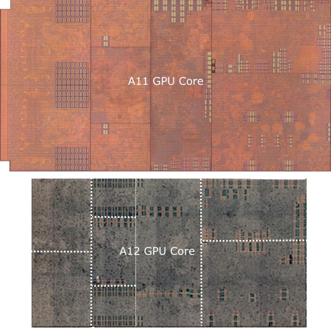
Credit: TechInsights Apple A12 Die Shot, ChipRebel Apple A11 Die Shot
Moving onto the A12 GPU – model named as the G11P, we see some very obvious similarities to last year’s A11 GPU. The individual function blocks seem to be largely located the same and constructed in a similar fashion.
What I think Apple’s biggest advancements in the A12 GPU is the fact that it now supports memory compression. I was very surprised to hear this during the announcement because at the same time it means two things: Prior Apple SoCs and their GPUs apparently didn’t have memory compression, and that now this alone should amount for a very significant boost in performance of the new GPU.
By memory compression, in particular we mean transparent framebuffer compression from the GPU to main memory. In the desktop space, vendors like Nvidia and AMD have had this for many years now, and it enabled the advancement of GPU performance even in the face of non-advancing memory-bandwidth increases. Smartphone GPUs also require memory compression, not only because of limited bandwidth on mobile SoCs, but most importantly because of the reduced power consumption that is associated with high bandwidth requirements. Arm’s AFBC has been the most publicly talked about mechanism in the mobile space, but other vendors such as Qualcomm or even Imagination have their own implementations.
Apple seems to be very late to the party in only introducing this with the A12 – however it also means the A12 will benefit from an unusually large generational boost in efficiency and performance, which makes a lot of sense given Apple’s proclaimed large increases for the new GPU.


253 Comments
View All Comments
Andrei Frumusanu - Saturday, October 6, 2018 - link
Eh no, it's single thread comparisons everywhere.Alistair - Saturday, October 6, 2018 - link
Thank you for making that clear. See my below comment with links, I put your data into a chart to compare. Is it fair to say IPC for the A12 in integers, is up to 64 percent faster?Hifihedgehog - Saturday, October 6, 2018 - link
Awesome! Thanks for the clarification. So my own education, is SPECint2006 a single-threaded test by its very nature? Can it be configured for multithreaded as well? If so, do you have multithreaded results forthcoming as well? I would love to see where Apple falls in this benchmark in that area as well.Andrei Frumusanu - Saturday, October 6, 2018 - link
SPECspeed is the score of running a single instance, SPECrate is running as many as there are cores on a system.It's not possible to run SPECrate on iOS anyhow without some very major hacky modifications of the benchmark because of the way it's ported without running in its own process. For Android devices it's possible, but I never really saw much interest or value for it.
Hifihedgehog - Saturday, October 6, 2018 - link
What about joules and watts? This is what is confusing me now. Something that seems a bit suspect to me is that the average energy and joule totals are not consistently lower together. That is, expect a device that has a lower average power usage to over the duration of the test to draw less total joules of energy. Mathematically speaking, I would naturally expect this especially in the case of higher benchmark scores since the lower power would be over a shorter space of time, meaning less total energy drawn.Andrei Frumusanu - Saturday, October 6, 2018 - link
The amount of Joules drawn depends on the average power and performance (time) of the benchmark.If a CPU uses 4 watts and gives 20 performance (say 5 minute to complete), it will use less energy than a CPU using 2 watts and giving 8 performance (12.5 minutes to complete), for example.
Dredd67 - Saturday, October 6, 2018 - link
I live in France and have to deal with intel radios since a while. I'm totally baffled to read all the comments about poor reception, dropped calls, wifi going crazy like this is news.This problem has been there since the beginning of Apple using intel chips ! It's just now that Americans have to use them also that it might finallybe adressed (please keep complaining, raise awareness, file a class action, whatever it takes) but you don't realize the pain these past years have been using an iphone elsewhere in the world...
For the record, I just gave my 7 (intel chip) to my daughter who broke here phone and reverted back to an old 6plus I kept for such cases (it also uses qualcomm). In the family I'm now the only only getting rock solid wifi, no dropped calls, consistent signal strenght, on a 4+ years old phone. And all this time I thought my carrier was messing around, my orbis were crap, or I just fumbled with my router settings.
Shame on you Apple, shame on you.
Oh and don't get me started on the camera: is this really what people want ? I think it's getting worse and worse, not better. Completely artifical images, looking more like cartoons than photographs. Same for Samsung and Google's phones. Hav a look at the P20 pro for a reality check. This is what photos should look like (contrast, colors - not really dependant on the sensor size).
Great review though.
ex2bot - Sunday, October 7, 2018 - link
The Halite app devs showed off an interesting technique they’re using or working on for the XS they call SmartRAW that may offer more control over the over saturation / lower contrast issues, etc.s.yu - Monday, October 8, 2018 - link
"Hav a look at the P20 pro for a reality check."?Your reality is the smeared textureless crap with oversharpening contours along object edges? Unbelievable.
serendip - Saturday, October 6, 2018 - link
Could these amazing CPU gains be translated to a midrange chip? Technically Android could run on Apple SoCs because they're all ARM licensed cores but porcines would gain flying abilities before that ever happened.It's too bad Android users are stuck with the best that ARM and Qualcomm can do, which isn't much compared to Apple's semi design team.