ATI Radeon X800 Pro and XT Platinum Edition: R420 Arrives
by Derek Wilson on May 4, 2004 10:28 AM EST- Posted in
- GPUs
The R420 Vertex Pipeline
The point of the vertex pipeline in any GPU is to take geometry data, manipulate it if needed (with either fixed function processes, or a vertex shader program), and project all of the 3D data in a scene to 2 dimensions for display. It is also possible to eliminate unnecessary data from the rendering pipeline to cut out useless work (via view volume clipping and backface culling). After the vertex engine is done processing the geometry, all the 2D projected data is sent to the pixel engine for further processing (like texturing and fragment shading).
The vertex engine of R420 includes 6 total vertex pipelines (R3xx has four). This gives R420 a 50% per clock increase in peak vertex shader power per clock cycle.
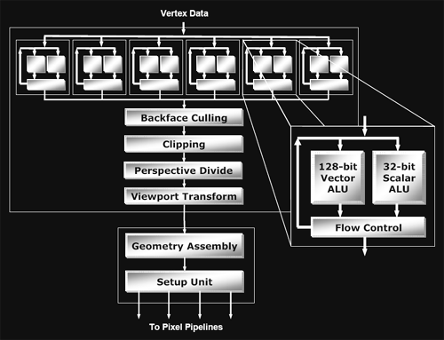
Looking inside an individual vertex pipeline, not much has changed from R3xx. The vertex pipeline is laid out exactly the same, including a 128bit vector math unit, and a 32bit scalar math unit. The major upgrade R420 has had from R3xx is that it is now able to compute a SINCOS instruction in one clock cycle. Before now, if a developer requested the sine or cosine of a number in a vertex shader program, R3xx would actually compute a taylor series approximation of the answer (which takes longer to complete). The adoption of a single cycle SINCOS instruction by ATI is a very smart move, as trigonometric computations are useful in implementing functionality and effects attractive to developers. As an example, developers could manipulate the vertices of a surface with SINCOS in order to add ripples and waves (such as those seen in bodies of water). Sine and cosine computations are also useful in more basic geometric manipulation. Overall, R420 has a welcome addition in single cycle SINCOS computation.
So how does ATI's new vertex pipeline layout compare to NV40? On a major hardware "black box" level, ATI lacks the vertex texture unit featured in NV40 that's required for shader model 3.0's vertex texturing support. Vertex texturing allows developers to easily implement any effect which would benefit from allowing texture data to manipulate geometry (such as displacement mapping). The other major difference between R420 and NV40 is feature set support. As has been widely talked about, NV40 supports Shader Model 3.0 and all the bells and whistles that come along with it. R420's feature set support can be described as an extended version of Shader Model 2.0, offering a few more features above and beyond the R3xx line (including more support of longer shader programs, and more registers).
What all this boils down to is that we are only seeing something that looks like a slight massaging of the hardware from R300 to R420. We would probably see many more changes if we were able too peer deeper under the hood. From a functionality standpoint, it is sometimes hard to see where performance comes from, but (as we will see even more from the pixel pipeline) as graphics hardware evolves into multiple tiny CPUs all laid out in parallel, performance will be effected by factors traditionally only spoken of in CPU analysis and reviews. The total number of internal pipeline stages (rather than our high level functionality driven pipeline), cache latencies, the size of the internal register file, number of instructions in flight, number of cycles an instructions takes to complete, and branch prediction will all come heavily into play in the future. In fact, this review marks the true beginning of where we will be seeing these factors (rather than general functionality and "computing power") determine the performance of a generation of graphics products. But, more on this later.
After leaving the vertex engine portion of R420, data moves into the setup engine. This section of the hardware takes the 2D projected data from the vertex engine, generates triangles and point sprites (particles), and partitions the output for use in the pixel engine. The triangle output is divided up into tiles, each of which are sent to a block of four pixel pipelines (called a quad pipeline by ATI). These tiles are simply square blocks of projected pixel data, and have nothing to do with "tile based rendering" (front to back rendering of small portions of the screen at a time) as was seen in PowerVR's Kyro series of GPUs.
Now we're ready to see what happens on the per-pixel level.


95 Comments
View All Comments
413xram - Wednesday, May 5, 2004 - link
They announced they where going to in there release anyway. Later on this summer. Why not now?jensend - Wednesday, May 5, 2004 - link
#61- nuts. 512 mb ram will pull loads more power, put out a lot more heat, cost a great deal more (especially now, since ram prices are sky-high), and give negligible if any performance gains. Heck, even 256 mb is still primarily a marketing gimmick.413xram - Wednesday, May 5, 2004 - link
They (ATI) are using the same technology that their previous cards are using. They pretty much just added more transistors to perform more functions at a higher speed. I am willing to bet my paycheck that they spent no where close to 400 million dollars to run neck and neck with nvidia in performance. I guess "virtually nothing" is an overstatement. My apologies.Phiro - Wednesday, May 5, 2004 - link
Where do you get your info that ATI spent "virtually nothing"?413xram - Wednesday, May 5, 2004 - link
Both cards perform brilliantly. They are truly a huge step in graphics processing. One problem I forsee though,is that Nvidia spent 400 million dollars into development of their new nv40 technology, while ATI spent virtually nothing to have the same performance gains. Economically that is a hard pill for Nvidia to swallow.It is true that Nvidia's card has the 3.0 pixel shading, unfortunatly though, they are banking on hardware that is not supported upon release of the card. In dealing with video cards from a consumers standpoint that is a hard sell. I have learned from the past that future possibilties of technology in hardware does nothing for me today. Not to mention the power supply issue that does not help neither.
Nvidia must find a way to get better performance out of their new card, I can't believe I'am saying that after seeing the specs that it already performs at, or it may be a long, HOT, and expensive summer for them.
P.S. Nvidia. A little advice. Speed up the release on your 512 mb card. That would definetly sell me. Overclocking your 6800 is something that 90% of us in this forum would do anyway.
theIrish1 - Wednesday, May 5, 2004 - link
heh, whatever.. whatever, and whatever. I love the fanboyisms....
I admit I am a fan of ATI cards. I bought a 9700pro and a 9500pro(in my secondary gaming rig) when they first came out, and an 8500 "pro" before that...but now I want to upgrade again. I am keeping an open mind. After looking at benchmarks, it is clear the both cards have their wins and losses depending on the test. I don't think there is a clear cut winner. nVidia got there by new innovation/technology. ATI got there by optimizing "older" technology.
At this point, with pricing being the same.. I think I still have to lean to the ATI cards. Main reasons being heat & power consumption. If the 6800U was $75 or $100 cheaper, I would probably go with that. It will be interesting to see where the 6850 falls benchmark wise, and also in pricing. If the 6850 takes the $500 pricepoint, where will that leave the 6800U? $450? Or with the 6850 be $550?
Something else about the x800Pro (which by the way, alot of the readers/posters seem to be getting confused as to what they are talking about between the Pro and XT models). Anyway, there are a few online stores out there taking pre-orders still for the x800PRO.... for $500+. I thought the Pro was going to go at $400 and the XT at $500...?!?
413xram - Wednesday, May 5, 2004 - link
Pumpkinierre - Wednesday, May 5, 2004 - link
On the fabrication o the two Gpus- the tech report:"Regardless, transistor counts are less important, in reality, than die size, and we can measure that. ATI's chips are manufactured by TSMC on a 0.13-micron, low-k "Black Diamond" process. The use of a low-capacitance dielectric can reduce crosstalk and allow a chip to run at higher speeds with less power consumption. NVIDIA's NV40, meanwhile, is manufactured by IBM on its 0.13-micron fab process, though without the benefit of a low-k dielectric."
The extra transistors of the 6800U might be taken up with the cinematic encoding/rendering embedded chip. Although ATI claim encoding in their X800p/XT blurb, I havent seen much yet to distinguish it from the 9800p in this field. The Tech report checked power consumption at the wall for their test systems and the 6800s ramp up the power a lot quicker with gpu speed so I'm not too hopeful about the overclock to 520Mhz and 6800u extreme gpu yields. Still, maybe a new stepping or 90nm SOI shrink might help (I noticed both manufacturers shied away from 90nm).
Anyway brilliant video cards from North America. Congratulations ATI and Nvidia!
NullSubroutine - Wednesday, May 5, 2004 - link
If it was nice sarcasm I can laugh, if it was nasty sarcasm you can back off. I can see it would be simple for me to overlook the map used, however no indication to what Atech used. One could assume or someone could ask for the real answer and if they are really lucky they will get a smart ass remark.After checking through 10 different reviews I found similar results to Atech when they had 25 bots, THG had none.
Next time save us both the hassle and just say THG didnt use bots, and Atech probably did.
TrogdorJW - Tuesday, May 4, 2004 - link
#54 - Think about things for a minute. Gee... I wonder why THG and AT got such different scores on UT2K4.... Might it be something like the selection of map and the demo used? Nah, that would be too simple. /sarcasmFrom THG: "For our tests in UT2004 we used our own timedemo on the map Assault-Torlan (no bots). All quality options are set to maximum."
No clear indication of what was used for the map or demo on AT, but I'm pretty sure that it was also a home-brewed demo, and likely on a different map and perhaps with a different number of players. Clearly, though, it was not the same demo as THG used... unless THG is in the habit of giving their benchmarking demos out? Didn't think so.
I see questions like this all the time. Unless two sites use the exact same settings, it's almost impossible to directly compare their scores. There is no conspiracy, though. Both sites pretty much say the same thing: close match, with the edge going to ATI right now, especially in DX9, while NV still reigns supreme in OGL.