Arm's Cortex-A76 CPU Unveiled: Taking Aim at the Top for 7nm
by Andrei Frumusanu on May 31, 2018 3:01 PM EST- Posted in
- CPUs
- Arm
- Smartphones
- Mobile
- SoCs
- Cortex-A76
Cortex A76 µarch - Frontend
Starting off with a rough overview of the Cortex A76 microarchitectural diagram we see the larger functional blocks. The A76 doesn’t look too different than other Arm processors in this regard and the differences come only with details that Arm is willing to divulge. To overly simplify it, this is a superscalar out-of-order core with a 4-wide decode front-end with 8 execution ports in the backend with a total implementation pipeline depth of 13 stages with the execution latencies of a 11 stage core.

In the front-end, Arm has created a new predict/fetch unit that it calls a “predict-directed fetch”, meaning the branch prediction unit feeds into the instruction fetch unit. This is a divergence from past Arm µarches and it allows for both higher performance and lower power consumption.

The branch prediction unit is what Arm calls a first in the industry in adopting a hybrid indirect predictor. The predictor is decoupled from the fetch unit and its supporting large structures operate separate from the rest of the machine – likely what this means is that it will be easier to clock-gate during operation to save on power. The branch predictor is supported by 3-level branch target caches; a 16-entry nanoBTB, a 64-entry microBTB and a 6000 entry main BTB. Arm claimed back in the A73 and A75 generations of branch predictors were able to nearly predict all taken branches so this new unit in the A76 seems to be one level above that in capability.
The branch unit operates at double the bandwidth of the fetch unit – it operates on 32B/cycle meaning up to 8 32b instructions per cycle. This feeds a fetch queue in front of the instruction fetch consisting of 12 “blocks”. The fetch unit operates at 16B/cycle meaning 4 32b instructions. The branch unit operating at double the throughput makes it possible to get ahead of the fetch unit. What this serves is that in the case of a mispredict it can hide branch bubbles in the pipeline and avoid stalling the fetch unit and the rest of the core. The core is said to able to cope with up to 8 misses on the I-side.
I mentioned at the beginning that the A76 is a 13-stage implementation with the latency of an 11-stage core. What happens is that in latency-critical paths the stages can be overlapped. One such cycle happens between the second cycle of the branch predict path and the first cycle of the fetch path. So effectively while there’s 4 (2+2) pipeline stages on the branch and fetch, the core has latencies of down to 3 cycles.
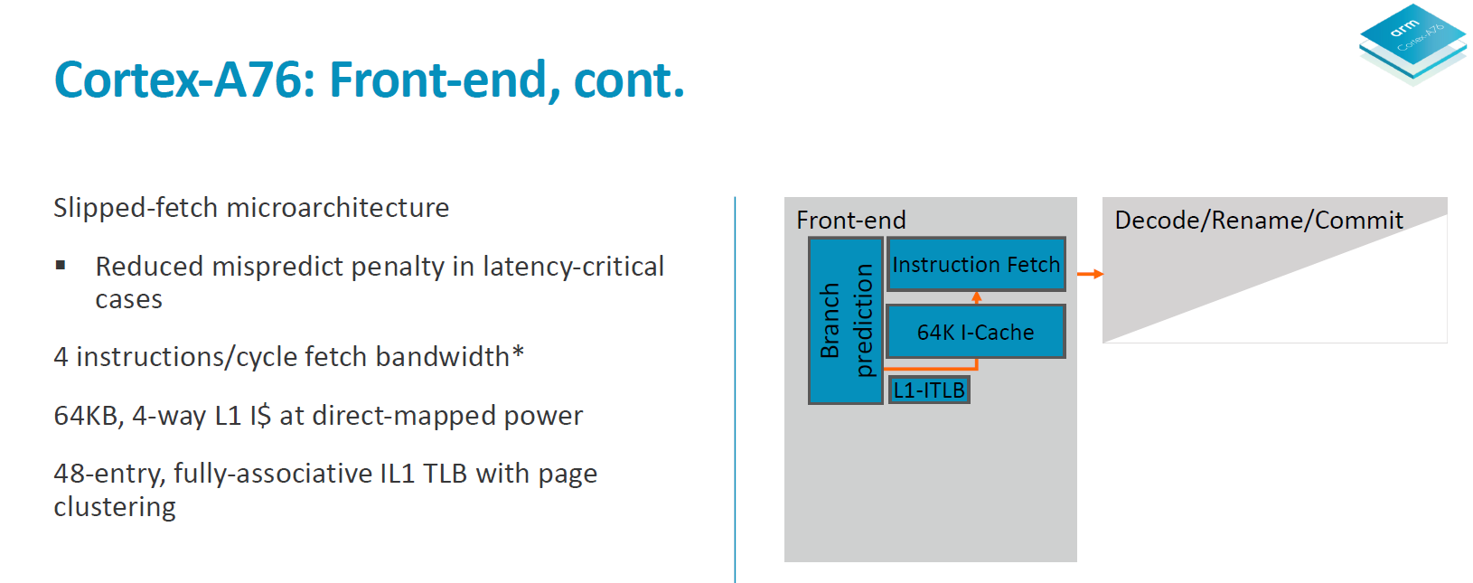
On the decode and rename stages we see a throughput of 4 instructions per cycle. The A73 and A75 were respectively 2 and 3-wide in their decode stages so the A76 is 33% wider than the last generation in this aspect. It was curious to see the A73 go down in decode width from the 3-wide A72, but this was done to optimise for power efficiency and “leanness” of the pipeline with goals of improving the utilisation of the front-end units. With the A76 going 4-wide, this is also Arms to date widest microarchitecture – although it’s still extremely lean when putting it into juxtaposition with competing µarches from Samsung or Apple.
The fetch unit feeds a decode queue of up to 16 32b instructions. The pipeline stages here consist of 2 cycles of instruction align and decode. It looks here Arm decided to go back to a 2-cycle decode as opposed to the 1-cycle unit found on the A73 and A75. As a reminder the Sophia cores still required a secondary cycle on the decode stage when handling instructions utilising the ASIMD/FP pipelines so Arm may have found other optimisation methods with the A76 µarch that warranted this design decision.
The decode stage takes in 4 instructions per cycle and outputs macro-ops at an average ratio of 1.06Mops per instruction. Entering the register rename stage we see heavy power optimisation as the rename units are separated and clock gated for integer/ASIMD/flag operations. The rename and dispatch are a 1 cycle stage which is a reduction from the 2-cycle rename/dispatch from the A73 and A75. Macro-ops are expanded into micro-ops at a ratio of 1.2µop per instruction and we see up to 8µops dispatched per cycle, which is an increase from the advertised 6µops/cycle on the A75 and 4µops/cycle on the A73.
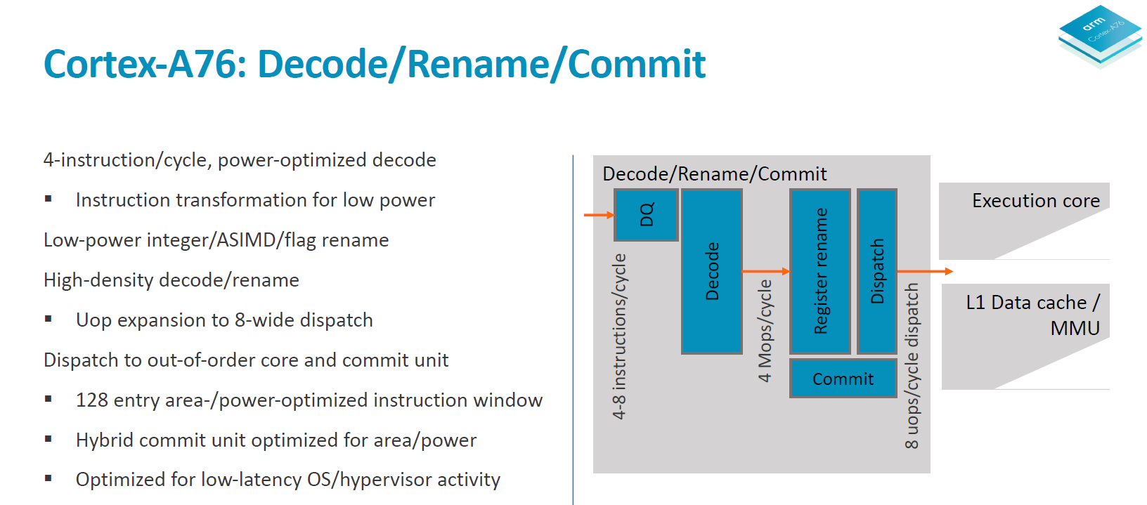
The out-of-order window commit size of the A76 is 128 and the buffer is separated into two structures responsible for instruction management and register reclaim, called a hybrid commit system. Arm here made it clear that it wasn’t focusing on increasing this aspect of the design as it found it as a terrible return on investment when it comes to performance. It is said that the performance scaling is 1/7th – meaning a 7% increase of the reorder buffer only results in a 1% increase in performance. This comes at great juxtaposition compared to for example Samsung's M3 cores with a very large 224 ROB.
As a last note on the front-end, Arm said to have tried to optimised the front-end for lowest possible latency for hypervisor activity and system calls, but didn’t go into more details.


123 Comments
View All Comments
lilmoe - Thursday, May 31, 2018 - link
Total power draw per workload is where it's at.Wardrive86 - Thursday, May 31, 2018 - link
Sustained performance is where it is at.lilmoe - Friday, June 1, 2018 - link
What does sustainable even mean anymore? Assuming you have proper power delivery, you can sustain 5-7w tdp on a smartphone. Doesn't mean it's efficient.Total power draw...... over time. All day.
erple2 - Friday, June 1, 2018 - link
I suspect you have to amend that with "with reasonable performance". If it takes all day to do something but sips negligible power to do so (thus power draw for that workload is small) isn't helpful if it's loading a web page.Wardrive86 - Thursday, May 31, 2018 - link
Sounds like a brilliant core! If it comes as fast as projected it MAY even drive Cortex A75 based devices' price down. It is incredible that even now they are still making great performance gains. Seems to me between A72 and A73 they got the "hard to get" performance and power metrics nailed down and now are enjoying the low lying fruit "i.e. going wider, increasing memory performance, etc." which is easier to attain just with process node advantagesserendip - Friday, June 1, 2018 - link
I thought the A73 had a different architecture than the A72 and it was slower on some tasks. The A76 is supposed to be a completely new design.I'm happy with my old 4x A53 + 2x A72 device. I would be happier with a 6x A55 + 2x A80, if ARM could come up with a hypothetical big and wide core that's similar to Monsoon but without the ridiculous power issues.
Wardrive86 - Friday, June 1, 2018 - link
Exactley, A72 was wider than A73 in the front and back ends, but performance was relatively the same. They got better power and about the same performance from a slimmer, leaner core...again seems to me like they went after the "hard to get" performance and power metricsvladx - Friday, June 1, 2018 - link
Sustained performance is loads better on A73 versus the A72.Wardrive86 - Saturday, June 2, 2018 - link
Agreed! Paid dividends on the A75 and surely the A76. Now they can enjoy the fruit of their laborporcupineLTD - Sunday, June 3, 2018 - link
This article seems to show exactly the opposite: https://www.anandtech.com/show/11088/hisilicon-kir...