Arm's Cortex-A76 CPU Unveiled: Taking Aim at the Top for 7nm
by Andrei Frumusanu on May 31, 2018 3:01 PM EST- Posted in
- CPUs
- Arm
- Smartphones
- Mobile
- SoCs
- Cortex-A76
Cortex A76 µarch - Frontend
Starting off with a rough overview of the Cortex A76 microarchitectural diagram we see the larger functional blocks. The A76 doesn’t look too different than other Arm processors in this regard and the differences come only with details that Arm is willing to divulge. To overly simplify it, this is a superscalar out-of-order core with a 4-wide decode front-end with 8 execution ports in the backend with a total implementation pipeline depth of 13 stages with the execution latencies of a 11 stage core.

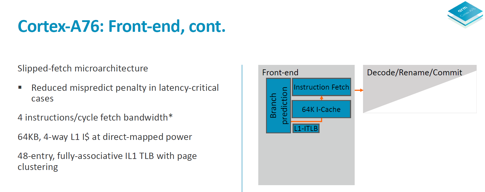
In the front-end, Arm has created a new predict/fetch unit that it calls a “predict-directed fetch”, meaning the branch prediction unit feeds into the instruction fetch unit. This is a divergence from past Arm µarches and it allows for both higher performance and lower power consumption.

The branch prediction unit is what Arm calls a first in the industry in adopting a hybrid indirect predictor. The predictor is decoupled from the fetch unit and its supporting large structures operate separate from the rest of the machine – likely what this means is that it will be easier to clock-gate during operation to save on power. The branch predictor is supported by 3-level branch target caches; a 16-entry nanoBTB, a 64-entry microBTB and a 6000 entry main BTB. Arm claimed back in the A73 and A75 generations of branch predictors were able to nearly predict all taken branches so this new unit in the A76 seems to be one level above that in capability.
The branch unit operates at double the bandwidth of the fetch unit – it operates on 32B/cycle meaning up to 8 32b instructions per cycle. This feeds a fetch queue in front of the instruction fetch consisting of 12 “blocks”. The fetch unit operates at 16B/cycle meaning 4 32b instructions. The branch unit operating at double the throughput makes it possible to get ahead of the fetch unit. What this serves is that in the case of a mispredict it can hide branch bubbles in the pipeline and avoid stalling the fetch unit and the rest of the core. The core is said to able to cope with up to 8 misses on the I-side.
I mentioned at the beginning that the A76 is a 13-stage implementation with the latency of an 11-stage core. What happens is that in latency-critical paths the stages can be overlapped. One such cycle happens between the second cycle of the branch predict path and the first cycle of the fetch path. So effectively while there’s 4 (2+2) pipeline stages on the branch and fetch, the core has latencies of down to 3 cycles.
On the decode and rename stages we see a throughput of 4 instructions per cycle. The A73 and A75 were respectively 2 and 3-wide in their decode stages so the A76 is 33% wider than the last generation in this aspect. It was curious to see the A73 go down in decode width from the 3-wide A72, but this was done to optimise for power efficiency and “leanness” of the pipeline with goals of improving the utilisation of the front-end units. With the A76 going 4-wide, this is also Arms to date widest microarchitecture – although it’s still extremely lean when putting it into juxtaposition with competing µarches from Samsung or Apple.
The fetch unit feeds a decode queue of up to 16 32b instructions. The pipeline stages here consist of 2 cycles of instruction align and decode. It looks here Arm decided to go back to a 2-cycle decode as opposed to the 1-cycle unit found on the A73 and A75. As a reminder the Sophia cores still required a secondary cycle on the decode stage when handling instructions utilising the ASIMD/FP pipelines so Arm may have found other optimisation methods with the A76 µarch that warranted this design decision.
The decode stage takes in 4 instructions per cycle and outputs macro-ops at an average ratio of 1.06Mops per instruction. Entering the register rename stage we see heavy power optimisation as the rename units are separated and clock gated for integer/ASIMD/flag operations. The rename and dispatch are a 1 cycle stage which is a reduction from the 2-cycle rename/dispatch from the A73 and A75. Macro-ops are expanded into micro-ops at a ratio of 1.2µop per instruction and we see up to 8µops dispatched per cycle, which is an increase from the advertised 6µops/cycle on the A75 and 4µops/cycle on the A73.
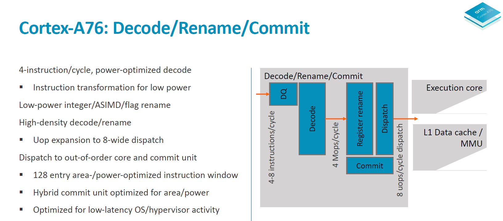
The out-of-order window commit size of the A76 is 128 and the buffer is separated into two structures responsible for instruction management and register reclaim, called a hybrid commit system. Arm here made it clear that it wasn’t focusing on increasing this aspect of the design as it found it as a terrible return on investment when it comes to performance. It is said that the performance scaling is 1/7th – meaning a 7% increase of the reorder buffer only results in a 1% increase in performance. This comes at great juxtaposition compared to for example Samsung's M3 cores with a very large 224 ROB.
As a last note on the front-end, Arm said to have tried to optimised the front-end for lowest possible latency for hypervisor activity and system calls, but didn’t go into more details.


123 Comments
View All Comments
iwod - Friday, June 1, 2018 - link
Even if Apple moved A11 from 10nm to 7nm, and runs at 3Ghz it will still be a huge gap in performance. Let alone they will have A12 and 7nm shipping in a few months time. Compare this to A76, which I don't think will come in 2018.So there is still roughly a 3 years gap between ARM and Apple in IPC or Single thread performance.
Lolimaster - Friday, June 1, 2018 - link
And why do you care about IPC, when 99.99% of all smartphone users:-Use the phone as a gloried clock
-A tool for showing off (even with the cancer "dynamic" profile on Samsung AMOLED powered devices, they don't know the "basic" calibrated profile exists)
-Twitter, facebook, instagram, whatapp
Where is your need for performance? Unless you buy a phone to run antutu/geekbench all the time you pick the phone out of your pockets.
The biggest improvement in phone performance was the jump from slow/high latency EMMC to nvme-like nand (apple), UFS for samsung and the others.
serendip - Friday, June 1, 2018 - link
Spot on. I've got a SD650 and a SD625 phone, one with A72 big cores and the other with only A53 cores, and for web browsing and chatting they're almost indistinguishable. The 625 device also has much better battery life.darwiniandude - Friday, June 1, 2018 - link
Of course a faster device can accomplish a task faster and drop back to idle power effciency to aid battery life. Depends on many factors, but running at (hypothetical) 20 units of performance per second over 5 seconds (total 100) then dropping back to idle might be preferable to 10 units of performance per second over 10 seconds.Also, remember Apple’s devices do much on device, the Kinect-like FaceID for one, and unlike Google Photos where images are scanned for content in the cloud (this picture contains a bridge, and a dog) iOS devices scan their libraries on device when on charge.
name99 - Friday, June 1, 2018 - link
That's like saying Intel shouldn't bother with performance any more because 99.99% of PCs run Facebook in the web browser, email, and Word.(a) Apple sells delight, and part of delight in your phone is NEVER waiting. If you want to save money, buy a cheaper phone and wait, but part of Apple's value proposition is that, for the money you spend, you reduce the friction of constant short waits. (Compare, eg, how much faster the phone felt when 1st gen TouchID was replaced with the faster 2nd TouchID. Same thing now with FaceID; it works and works well. But it will feel even smoother when the current half second delay is dropped to a tenth of a second [or whatever].)
(b) Apple chips also go into iPads. And people use iPads (and sometimes iPhones) for more than you claim --- for various artistic tasks (manipulating video and photos, drawing with very fancy [ie high CPU] "brushes" and effects, creating music, etc). One of the reasons these jobs are done on iPads (and sometimes Surfaces) and not Android is because they need a decent CPU.
(c) Ambition. BECAUSE Apple has a decent CPU, they can put that CPU into their desktops. And, soon enough, also into their data centers...
serendip - Friday, June 1, 2018 - link
I'm curious about all this because I'm an iPad user. No iPhones though. Even an old iPad Mini is smoother than top Android tablets today.Does the CPU spike up to maximum speed quickly when loading apps or PDFs, then very quickly throttle down to minimum? I don't know how Apple make their UI so smooth while also having good battery life.
varase - Saturday, June 2, 2018 - link
Smooth is the iPhone X.When you touch the screen, touch tracking boosts to 120hz, even though they can only run the OLED screen at 60hz.
As for PDFs, MacOS (and as a consequence iOS) uses non-computational postscript as their graphics framework ... and PDF is essentially journaled postscript (like a PICT was journaled QuickDraw).
As for throttling down: yeah, when you've completed your computationally expensive task you throttle down to save power.
YaleZhang - Friday, June 1, 2018 - link
Reducing latency of floating point instructions from 3 cycles to 2 seems quite an accomplishment. For Intel, it's been >= 3 cycles (http://www.agner.org/optimize/instruction_tables.p...Skylake: 4 cycles / 4.3 GHz = 0.93 ns
A76: 2 cycles / 3 GHz = 0.66 ns
Skylake latency increased to 4 probably to achieve a higher clock, but if A76 can do it in 3, then Skylake should also be able to do it (3 cycles / 4.3 GHz) = 0.70 ns.
How did ARM do this?
tipoo - Tuesday, September 4, 2018 - link
Lower max clocks, shorter pipeline maybe?Quantumz0d - Friday, June 1, 2018 - link
Hilarious commenters. Apple's SoC ? Again ? I guess people need to think about how bad their Power envelope is. Their A11 gets beaten by 835 in consistency, dropping to 60% of clocks lol. And the battery killing SoC yes the battery capacity is less on iPhones. But Apple's R&D and the chips costs are very high vs the ARM. Not to forget how 845s GPU performance slaps and drowns that Custom *cough cough *Imagination* IP derived GPU core.They rely on the Single Thread performance because of power and optimization it goes for one OS and one HW ecosystem ruled and locked by Apple only where as ARM derived designs or Qcomm are robust for supporting wider hardware pool and can even run Windows OS.