Sizing Up Servers: Intel's Skylake-SP Xeon versus AMD's EPYC 7000 - The Server CPU Battle of the Decade?
by Johan De Gelas & Ian Cutress on July 11, 2017 12:15 PM EST- Posted in
- CPUs
- AMD
- Intel
- Xeon
- Enterprise
- Skylake
- Zen
- Naples
- Skylake-SP
- EPYC
Intel Expanding the Chipset: 10 Gigabit Ethernet and QuickAssist Technology
The refresh strategy from Intel on the chipset side has an ultra-long cadence. In recent memory, Intel’s platform launches are designed to support two generations of processor release, and in that time there is typically no chipset update, leaving the platform controller hub semi-static for functionality for usually three years. This is compared to the consumer side, where new chipsets are launched with every new CPU generation, with bigger jumps coming every couple of years. For the new launch today, Intel pushing the enterprise chipset ahead in a new direction.
The point of the chipset previously was to provide some basic IO support in the form of SATA/SAS ports, some USB ports, and a few PCIe lanes for simple controllers like USB 3.0, Gigabit Ethernet, or perhaps an x4 PCIe slot for a non-accelerator type card. The new chipsets, part of the C620 family codenamed Lewisburg, are designed to assist with networking, cryptography, and act more like a PCIe switch with up to 20 PCIe 3.0 lane support.
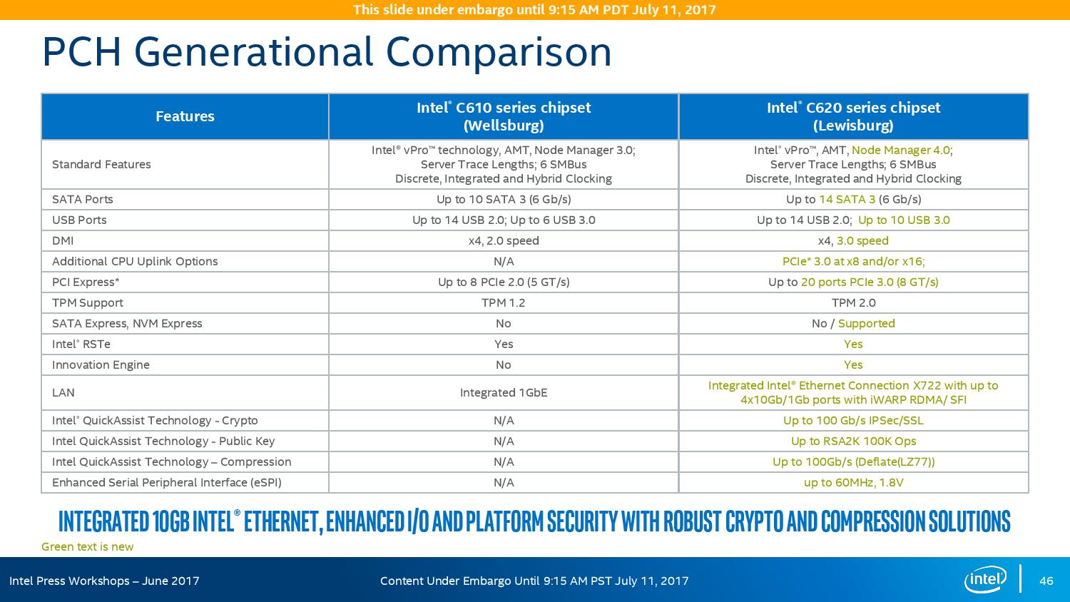
The headline features that matter most is the upgrade in DMI connection to the chipset, upgraded from DMI 2.0 to DMI 3.0 to match the consumer platforms, having those 20 PCIe 3.0 lanes from the chipset, and also the new feature under CPU Uplink.
For the new generation of Lewisburg chipsets, if an OEM requires that a platform has access to a cryptography engine or 10 Gigabit Ethernet, then they can attach 8 or 16 lanes from the processor into the chipset via this CPU Uplink port. Depending on which model of chipset is being used, this can provide up to four 10 GbE ports with iWARP RDMA, or up to 100 GB/s IPSec/SSL of QuickAssist support.
Intel will offer seven different versions of the chipset, varying in 10G and QAT support, but also varying in TDP:
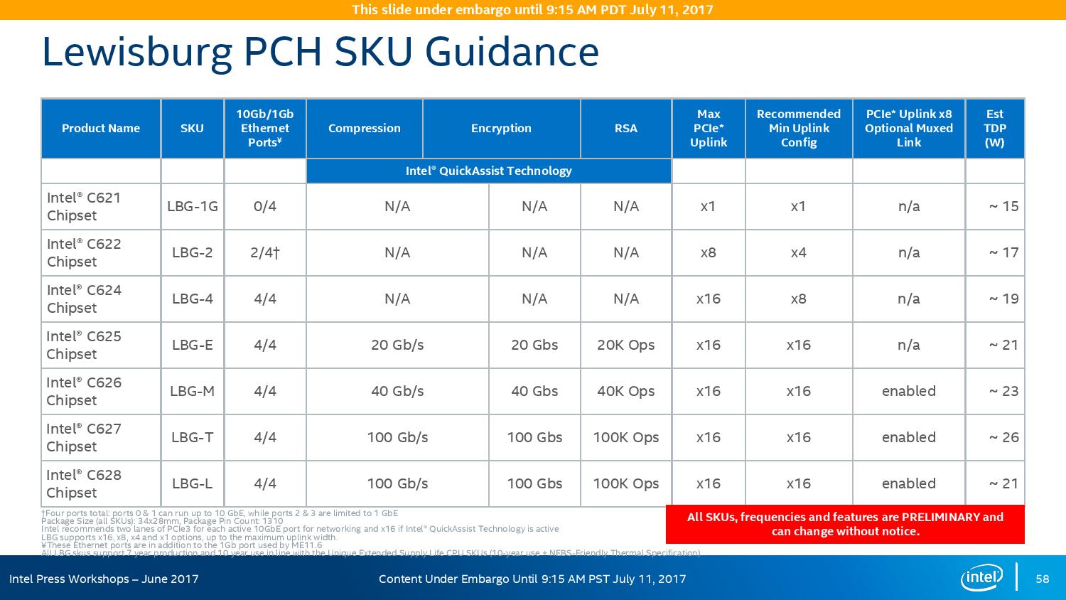
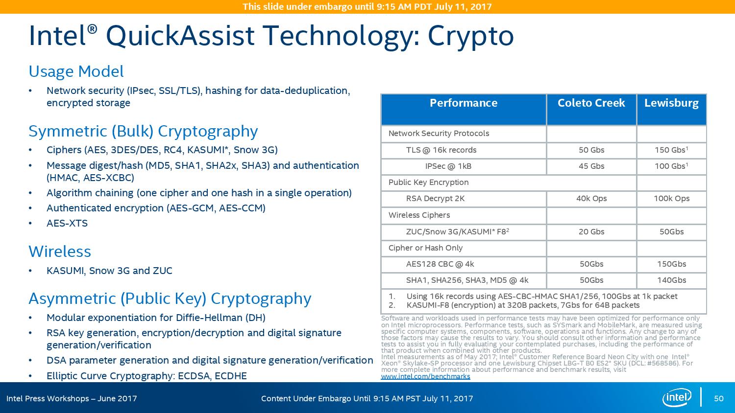
On the cryptography side, Intel has previously sold add-in PCIe cards for QuickAssist, but is now moving it onto the systems directly. By adding it into the chipset, it can be paired with the Ethernet traffic and done in-situ, and specifically Intel points to bulk cryptography (150 Gb/s AES256/SHA256), Public Key Encryption (100k ops of RSA2048) and compression (100+ Gb/s deflate).
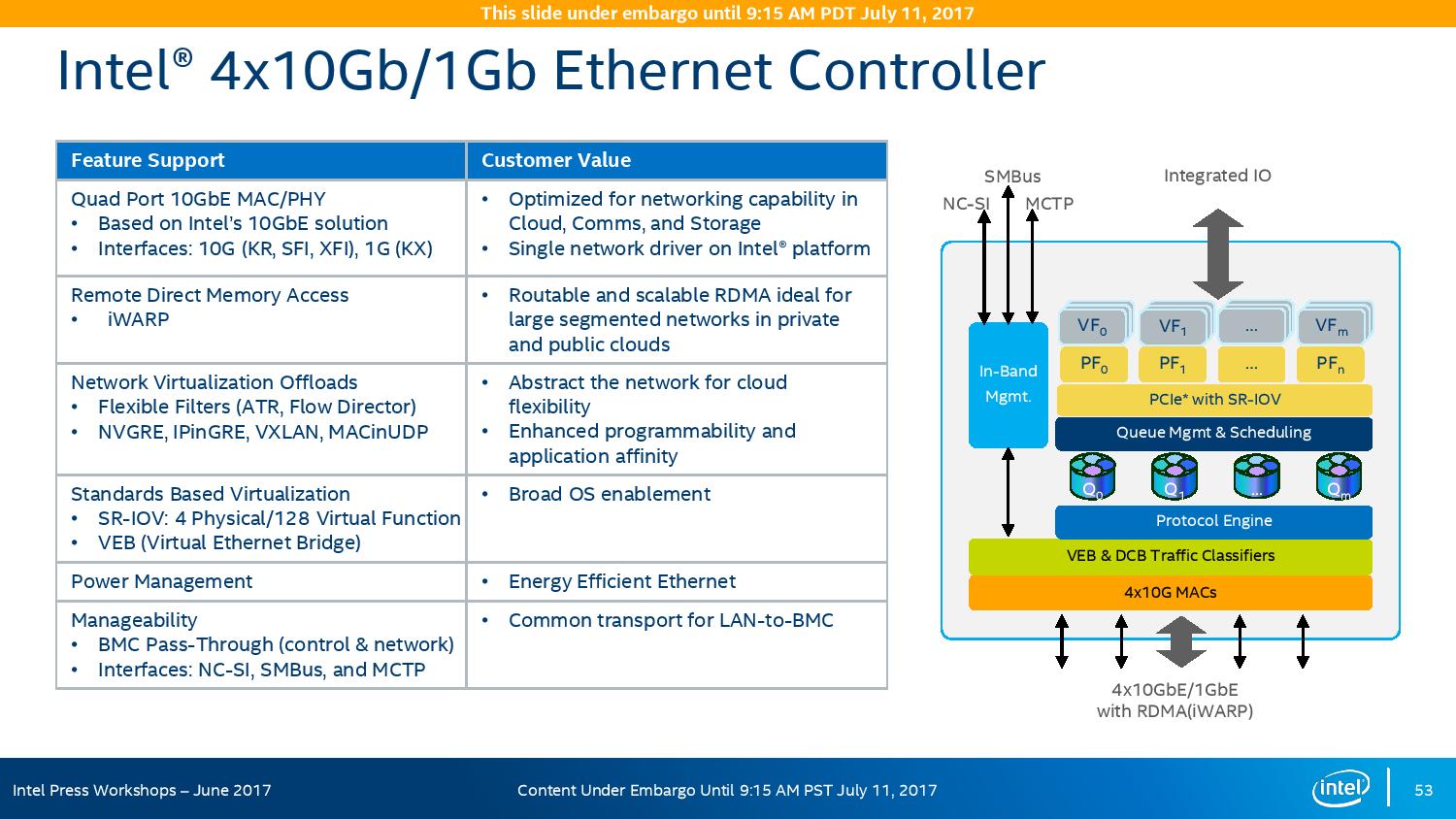
With the GbE, Intel has designed this to be paired with the X722 PHY, and supports network virtualization, traffic shaping, and supports Intel’s Data Plane Development Kit for advanced packet forwarding.
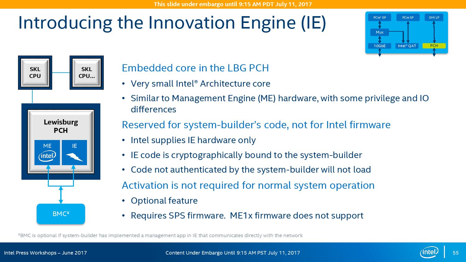
The chipset will also include a new feature called Intel’s Innovation Engine, giving a small embedded core into the PCH which mirrors Intel’s Management Engine but is designed for system-builders and integrators. This allows specialist firmware to manage some of the capabilities of the system on top of Intel’s ME, and is essentially an Intel Quark x86 core with 1.4MB SRAM.
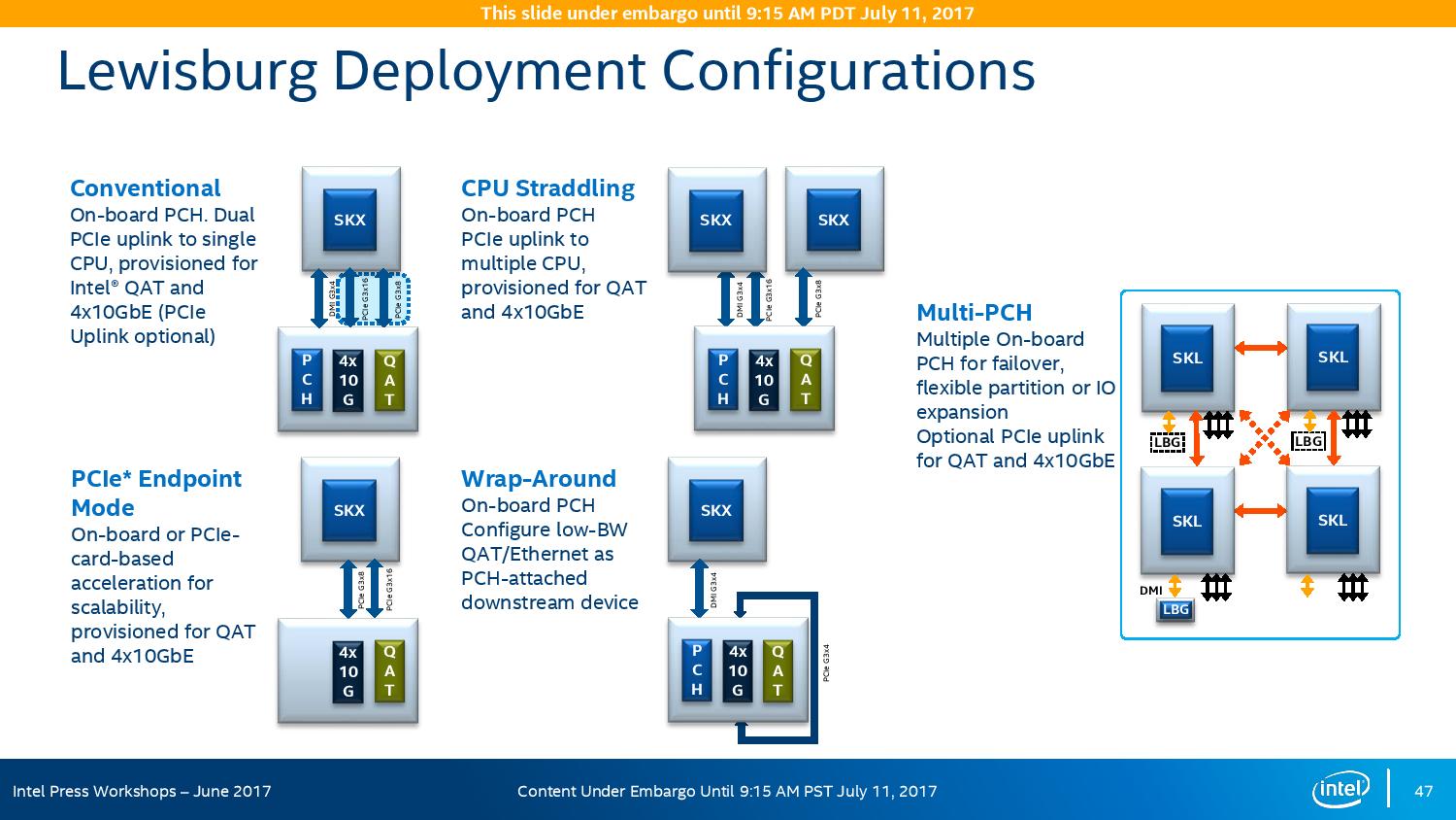
The chipsets are also designed to be supported between different CPUs within the same multi-processor system, or for a system to support multiple chipsets at once as needed.


219 Comments
View All Comments
psychobriggsy - Tuesday, July 11, 2017 - link
Indeed it is a ridiculous comment, and puts the earlier crying about the older Ubuntu and GCC into context - just an Intel Fanboy.In fact Intel's core architecture is older, and GCC has been tweaked a lot for it over the years - a slightly old GCC might not get the best out of Skylake, but it will get a lot. Zen is a new core, and GCC has only recently got optimisations for it.
EasyListening - Wednesday, July 12, 2017 - link
I thought he was joking, but I didn't find it funny. So dumb.... makes me sad.blublub - Tuesday, July 11, 2017 - link
I kinda miss Infinity Fabric on my Haswell CPU and it seems to only have on die - so why is that missing on Haswell wehen Ryzen is an exact copy?blublub - Tuesday, July 11, 2017 - link
Your actually sound similar to JuanRGA at SAKevin G - Wednesday, July 12, 2017 - link
@CajunArson The cache hierarchy is radically different between these designs as well as the port arrangement for dispatch. Scheduling on Ryzen is split between execution resources where as Intel favors a unified approach.bill.rookard - Tuesday, July 11, 2017 - link
Well, that is something that could be figured out if they (anandtech) had more time with the servers. Remember, they only had a week with the AMD system, and much like many of the games and such, optimizing is a matter of run test, measure, examine results, tweak settings, rinse and repeat. Considering one of the tests took 4 hours to run, having only a week to do this testing means much of the optimization is probably left out.They went with a 'generic' set of relative optimizations in the interest of time, and these are the (very interesting) results.
CoachAub - Wednesday, July 12, 2017 - link
Benchmarks just need to be run on as level as a field as possible. Intel has controlled the market so long, software leans their way. Who was optimizing for Opteron chips in 2016-17? ;)theeldest - Tuesday, July 11, 2017 - link
The compiler used isn't meant to be the the most optimized, but instead it's trying to be representative of actual customer workloads.Most customer applications in normal datacenters (not google, aws, azure, etc) are running binaries that are many years behind on optimizations.
So, yes, they can get better performance. But using those optimizations is not representative of the market they're trying to show numbers for.
CajunArson - Tuesday, July 11, 2017 - link
That might make a tiny bit of sense if most of the benchmarks run were real-world workloads and not C-Ray or POV-Ray.The most real-world benchmark in the whole setup was the database benchmark.
coder543 - Tuesday, July 11, 2017 - link
The one benchmark that favors Intel is the "most real-world"? Absolutely, I want AnandTech to do further testing, but your comments do not sound unbiased.