Exploring DynamIQ and ARM’s New CPUs: Cortex-A75, Cortex-A55
by Matt Humrick on May 29, 2017 12:00 AM EST- Posted in
- Smartphones
- CPUs
- Arm
- Mobile
- Cortex
- DynamIQ
- Cortex A75
- Cortex A55
DynamIQ
Before we discuss the new CPUs, we need to discuss DynamIQ. Introduced 5 years ago, ARM’s original big.LITTLE (bL) technology, which allows multiple clusters of up to 4 CPUs to be chained together, has been massively successful in the marketplace, allowing various combinations of its Cortex-A family of CPUs to power mobile devices ranging from the budget-friendly with no frills to the budget-busting flagships stuffed with technology. The combination of Cortex-A and bL extends beyond smartphones and tablets too, with applications ranging from servers to automotive.
Over the years, ARM’s IP and the needs of its customers have evolved, necessitating a new version of bL: DynamIQ. ARM started working on DynamIQ in 2013 by asking a single question: “How do you make big.LITTLE better?” Looking forward, ARM could see DynamIQ needed to be more flexible, more scalable, and offer better performance. Considering how much work went into this project, DynamIQ will be around for at least the next few years, so hopefully it delivers on those goals.
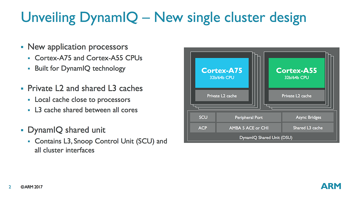
Like bL, DynamIQ provides a way to group CPUs into clusters and connect them to other processors and hardware within the system; however, there’s several significant changes, starting with the ability to place big and little Cortex-A CPUs in the same cluster. With bL, different CPUs had to reside within separate clusters. What appears to be a simple reshuffling of cores actually impacts CPU performance and configuration flexibility.
Another big change is the ability to place up to 8 CPUs inside a single cluster (up from 4 for bL), with the total number of CPUs scaling up to 256 with 32 clusters, which can scale even further to 1000s of CPUs with multi-chip support provided via a CCIX interface. Within a cluster CPUs are divided into voltage/frequency domains, and within a domain each core is inside its own power domain. This allows each CPU to be individually powered down, although all CPUs in the same domain must operate at the same frequency, which is no different from bL; however, with DynamIQ each cluster can support up to 8 voltage/frequency domains, providing greater flexibility than bL’s single voltage/frequency domain per cluster. So, what does this mean? It means that, in theory, an SoC vendor could place each CPU into its own voltage domain so that voltage/frequency could be set independently for each of the 8 CPUs in the cluster. Each voltage/frequency domain requires its own voltage regulator, which adds cost and complexity, so we’ll most likely continue to see 2-4 CPUs per domain.
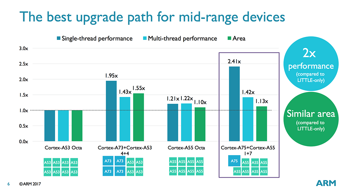
ARM still sees 8-core configurations being used in mobile devices over the next few years. With bL, this would likely be a 4+4 pairing using 4 big cores and 4 little cores or 8 little cores spread across 2 clusters. With DynamIQ, all 8 cores can fit inside a single cluster and can be split into any combination (1+7, 2+6, 3+5, 4+4) of A75 and A55 cores. ARM sees the 1+7 configuration, where one A55 core is replaced by a big A75 core, as particularly appealing for the mid-range market, because it offers up to 2.41x better single-thread performance and 1.42x better multi-thread performance for only a 1.13x increase in die area compared to an octa-core A53 configuration (iso-process, iso-frequency).
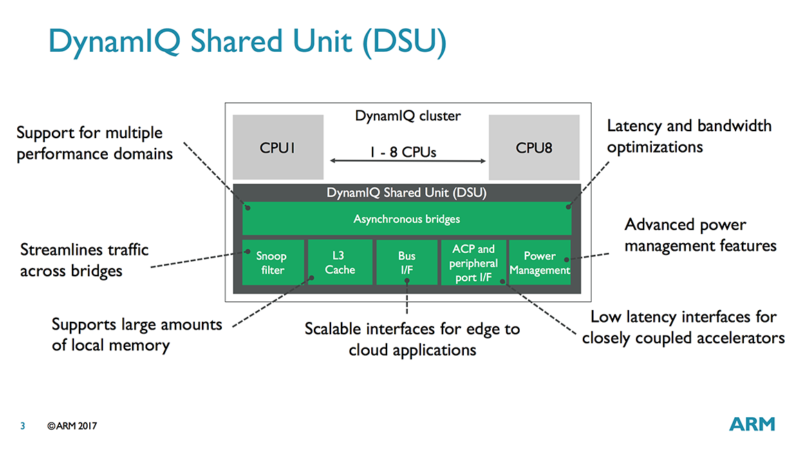
The main puzzle piece that enables this flexibility is the DynamIQ Shared Unit (DSU), a separate block that sits inside each DynamIQ cluster and functions as a central hub for the CPUs within the cluster and the bridge to the rest of the system. Each voltage/frequency domain in the cluster can be configured to run synchronously or asynchronously with the DSU. Using asynchronous bridges (one per domain) allows different CPUs (A75/A55) to operate at different frequencies (using synchronous bridges would force all CPUs to operate at the same frequency).
The DSU communicates with a CCI, CCN, or CMN cache-coherent interconnect through 1 to 2 128-bit AMBA 5 ACE ports or a single 256-bit AMBA 5 CHI port. There’s also an Accelerated Coherency Port (ACP) for attaching specialized accelerators that require cache coherency with the CPUs. It’s also used for enabling DynamIQ’s cache stashing feature, which we’ll discuss in a minute. Finally, there’s a separate peripheral port that’s used to program the accelerators attached to the ACP interface (basically a shortcut for programming transactions so they do not need to be routed through the system interconnect).
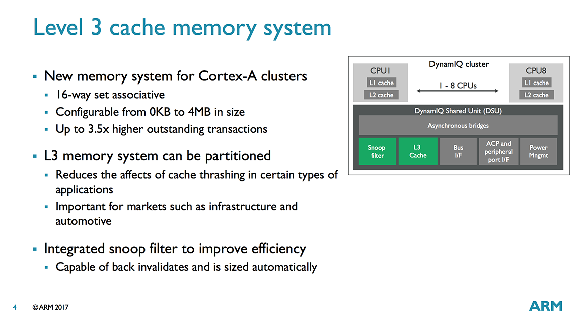
So far we’ve discussed DynamIQ’s flexibility and scalability features, but it also improves CPU performance through a new cache topology. With bL, CPUs inside a cluster had access to a shared L2 cache; however, DynamIQ compatible CPUs (currently limited to A75/A55) have private L2 caches that operate at the CPU core’s frequency. Moving the L2 closer to the core improves L2 cache latency by 50% or more. DynamIQ also adds another level of cache: The optional shared L3 cache lives inside the DSU and is 16-way set associative. Cache sizes are 1MB, 2MB, or 4MB, but may be omitted for certain applications like networking. The L3 cache is technically pseudo-exclusive, but ARM says it’s really closer to being fully-exclusive, with nearly all of the L3’s contents not appearing in the L2 and L1 caches. If the new L3 cache was inclusive, meaning that it contained a copy of a CPU’s L2, then its performance benefit would be largely mitigated and a lot of area and power would be wasted.
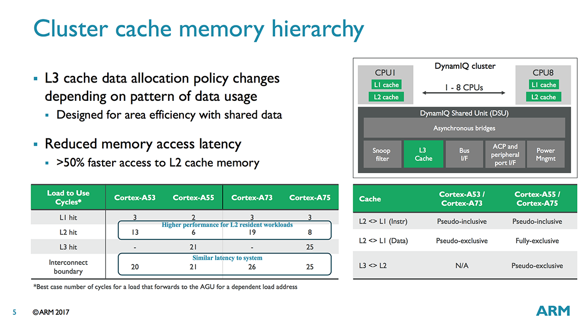
The L3 cache can be partitioned, which can be useful for networking or embedded systems that run a fixed workload or applications that require more deterministic data management. It can be partitioned into a maximum of 4 groups, and the split can be unbalanced, so 1 CPU could get 3MB while the other 7 CPUs would share the remaining 1MB in an 8-core 4MB L3 configuration. Each group can be assigned to specific CPU(s) or external accelerators attached to the DSU via the ACP or other interface. Any processors not specifically assigned to a cache group share the remaining L3 cache. The partitions are dynamic and can be created/adjusted during runtime by the OS or hypervisor.
One of the features supported by DynamIQ is error reporting, which allows the system to report detected errors, both correctable and uncorrectable, to software. The L3 supports ECC/parity (actually all levels of cache and snoop filters do, with SECDED on caches that can hold dirty data and SED parity on caches that only hold clean data) in order to be ASIL-D compliant. The L3 also has persistent error correction and can support recovery from a single hard error (data poisoning is supported at a 64-bit granularity).
Another new feature is cache stashing, which allows a GPU or other specialized accelerators and I/O agents to read/write data into the shared L3 cache or directly into a specific CPU’s L2 cache via the ACP or AMBA 5 CHI port. A specific example is a networking appliance that uses a TCP/IP offload engine to accelerate packet processing. Instead of writing its data to system memory for the CPU to fetch or relying on some other cache coherency mechanism, the accelerator could use cache stashing to write its data directly into the CPU’s L2, increasing performance and reducing power consumption.
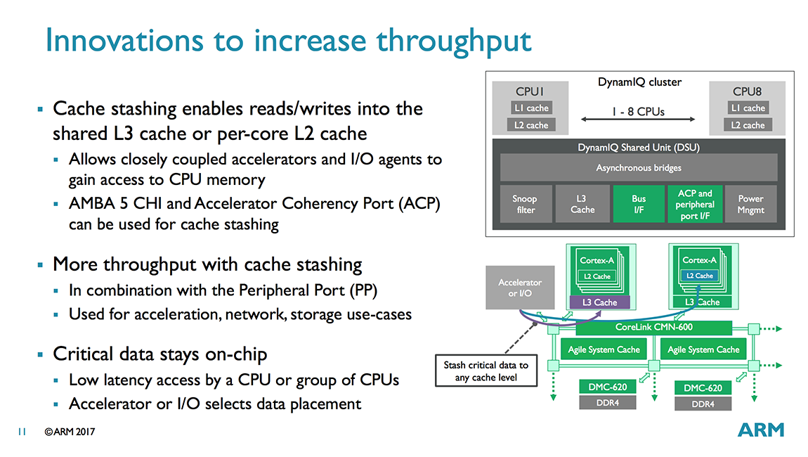
In order to use cache stashing, the software drivers running in kernel space need to be aware of the processor and cache topology, which will require custom code to enable hardware outside the cluster to access the shared L3 or an individual CPU’s L2. While a limitation for consumer electronics where time to market is key, it’s not as serious of an issue for commercial applications.
While cache stashing could be a useful feature for sharing data with processors sitting outside the cluster, DynamIQ also makes it easier to share data among CPUs within a cluster. This is one of the reasons why ARM wanted to bring big and little CPUs into the same cluster. Moving cache lines within a DynamIQ cluster is faster than moving them between clusters like with bL, reducing latency when migrating threads between big and little cores.

DynamIQ also includes improved power management. Having the DSU perform all cache and coherency management in hardware instead of software saves several steps when changing CPU power states, allowing the CPU cores to power up or down much faster than before with bL. The DSU can also power down portions of the L3 cache to reduce leakage power by autonomously monitoring cache usage and switching between full on, half off, and full off states.
The DSU includes a Snoop Control Unit (SCU) with an integrated snoop filter for handling the new cache topology. Together with L3 cache and other control logic, the DSU is about the same area as an A55 core in its max configuration or half the area of an A55 in its min configuration. These are just rough estimates because most of the DSU area is used by the L3 cache and the size of the DSU logic scales with the number of CPU cores.
Some of ARM’s partners may be slow to migrate from bL to DynamIQ, choosing to stick with a technology and CPU cores they are familiar with instead of investing the extra time and money required to develop new solutions. But for performance (and marketing) sensitive markets that need access to ARM’s latest CPU cores, such as mobile, the switch to DynamIQ should happen quickly, with the first DynamIQ SoCs likely to appear by the end of 2017 or early 2018.


104 Comments
View All Comments
melgross - Wednesday, May 31, 2017 - link
No, we don't know if they're fake. TSMC stated, months ago, that they were delivering 10nm parts to their largest customers, which one would presume, is Apple.And my statement stand. If the best the u35 can do is just over 2,000, then these parts are slightly over twice as fast. And if the claim for the multiprocessing score is right, then that's well over the score for any 4 core ARM chip from anyone else.
''Traditionally", these scores that leak out, whether real, or not, are remarkably close to what's tested after Apple's product does come out, often being somewhat lower that the "real" scores.
jjj - Monday, May 29, 2017 - link
Apple's ST perf is marketing for folks like you, nothing more.ST perf is too high for mobile even with A75 and ST perf is not what matters. We would all be better off with less ST and higher efficiency.
Sadly people like you are pushing the industry into pushing ST for no reason.
Apple 's core is huge compared to ARM's core and for what, ST perf you don't need ,lower MT and efficiency.
aryonoco - Monday, May 29, 2017 - link
I'm curious to know what you are basing this on.From where I stand, the great majority of times on mobiles are spent either on the web, or in games. Javascript is still very much single-threaded, so higher ST performance directly results in better web experience.
Why do you think that "I don't need ST perf"?
Note: I don't have a single iOS device, though I'd have loved to have an Android device with A10 inside.
melgross - Wednesday, May 31, 2017 - link
Nonsense! If this were a Qualcomm or Samsung chip, you wouldn't be saying that, and we both know that. While I don't know what other chips use, Apple's is about 3 watts, which is likely about what the others are. But Apple manages to get far better performance. That's never a bad thing.I don't think you understand what smartphones are being used for.
melgross - Monday, May 29, 2017 - link
While we don't know if the benchmarks that have been listed for the new A11 from Apple are real, though they seem to be what we would expect, individual cores are hitting over 4,500 and slightly under 9,000 multicore, with both cores.With everything I've read here, I'm still not sure what we would expect from these parts. The highest performing ARM used on Android seems to be well below 2,000 per core, with almost 7,000 for 4 core multicore.
So, what's to expect here? And how much of this advantage is coming from the process shrink, rather than from core improvements?
tipoo - Monday, May 29, 2017 - link
Yeah that's what I'm wondering, how much is IPC improvement and how much is just clocking it higher on a new node.Wardrive86 - Monday, May 29, 2017 - link
Shouldn't that be 2-128 bit NEON/FPU pipelines for the A75? If not that's a Max 4 flops per clock and lower than the cores it is replacingserendip - Monday, May 29, 2017 - link
I hope chip vendors don't push 8x A55 designs for the midrange because they're only good for the low end. Having so many similar cores is pointless because Android rarely uses all 8 cores.I'd rather see more 2+4 or 4+4 designs with the A55 and A75, especially something like the old Snapdragon 650/652 with the latest cores and processes. I'm looking to upgrade my Mi Max a year from now and the relevant chips should appear by then. On the other hand, with constant driver updates, this phone could last for a few years still.
Wilco1 - Tuesday, May 30, 2017 - link
A Cortex-A55 at 2.5GHz (same as Helio P25) would get close to ST performance of Galaxy S6 (and match MT perf). That was top-end 2 years ago... So while I agree 1+7 or 2+6 would be much better than 8x A55, I don't think you could call an S6 a low-end phone even in 2018!serendip - Tuesday, May 30, 2017 - link
The Helios with their decacore design couldn't beat the real world speed and battery life of a Snapdragon 65x. It's foolish to run an A55 at 2.5 GHz when an A75 at lower speed uses similar amounts of power while being much faster. At one point, you move the load from the donkey and put it on a race horse :)