The Intel Optane SSD DC P4800X (375GB) Review: Testing 3D XPoint Performance
by Billy Tallis on April 20, 2017 12:00 PM ESTMixed Read/Write Performance
Workloads consisting of a mix of reads and writes can be particularly challenging for flash based SSDs. When a write operation interrupts a string of reads, it will block access to at least one flash chip for a period of time that is substantially longer than a read operation takes. This hurts the latency of any read operations that were waiting on that chip, and with enough write operations throughput can be severely impacted. If the write command triggers an erase operation on one or more flash chips, the traffic jam is many times worse.
The occasional read interrupting a string of write commands doesn't necessarily cause much of a backlog, because writes are usually buffered by the controller anyways. But depending on how much unwritten data the controller is willing to buffer and for how long, a burst of reads could force the drive to begin flushing outstanding writes before they've all been coalesced into optimal sized writes.
The effect of a read still applies to the Optane SSD's 3D XPoint memory, but with greatly reduced severity. Whether a block of reads coming in has an effect depends on how the Optane SSD's controller manages the 3D XPoint memory.
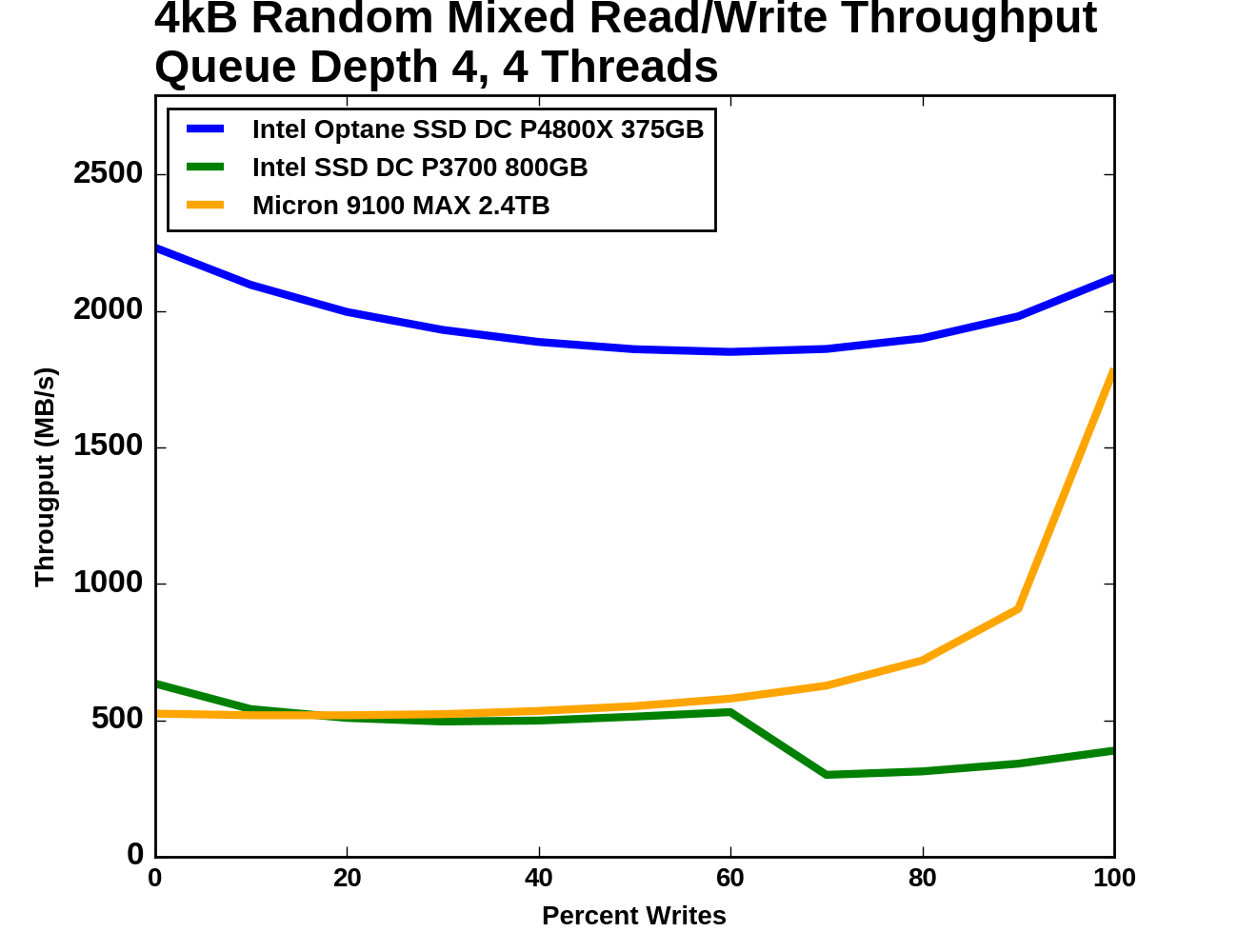
Queue Depth 4
Our first mixed workload test is an extension of what Intel describes in their specifications for throughput of mixed workloads. A total queue depth of 16 is achieved using four worker threads, each performing a mix of random reads and random writes. Instead of just testing a 70% read mixture, the full range from pure reads to pure writes is tested at 10% increments.
 |
|||||||||
| Vertical Axis units: | IOPS | MB/s | |||||||
The Optane SSD's throughput does indeed show the bathtub curve shape that is common for this sort of mixed workload test, but the sides are quite shallow and the minimum (at 40% reads/60% writes) is still 83% of the peak throughput (which occurs with the all-reads workload). While the Optane SSD is operating near 2GB/s the flash SSDs spend most of the test only slightly above 500MB/s. When the portion of writes increases to 70%, the two flash SSDs begin to diverge: the Intel P3700 loses almost half its throughput and only recovers a little of it during the remainder of the test, while the Micron 9100 begins to accelerate and comes much closer to the Optane SSD's level of performance.
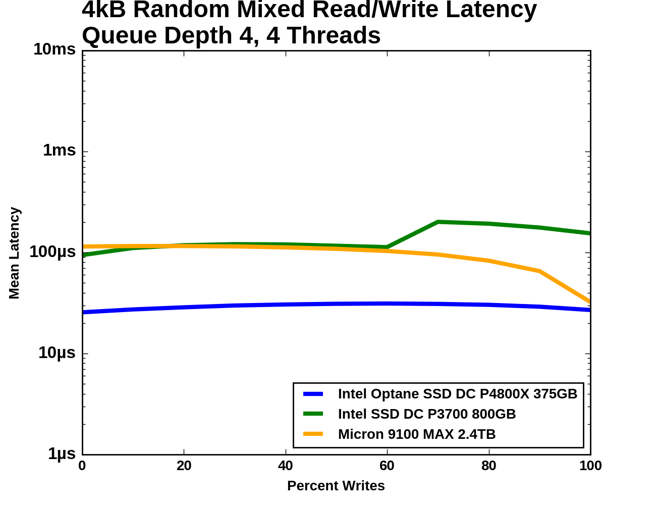 |
|||||||||
| Mean | Median | 99th Percentile | 99.999th Percentile | ||||||
The median latency curves for the two flash SSDs show a substantial drop when the median operation switches from a read to a cacheable write. The P3700's median latency even briefly drops below that of the Optane SSD, but then the Optane SSD is handling several times the throughput. The 99th and 99.999th percentile latencies for the Optane SSD are relatively flat after jumping a bit when writes are first introduced to the mix. The flash SSDs have far higher 99th and 99.999th percentile latencies through the middle of the test, but much fewer outliers during the pure read and pure write phases.
Adding Writes to a Drive that is Reading
The next mixed workload test takes a different approach and is loosely based on the Aerospike Certification Tool. The read workload is constant throughout the test: a single thread performing 4kB random reads at QD1. Threads performing 4kB random writes at QD1 and throttled to 100MB/s are added to the mix until the drive's throughput is saturated. As the write workload gets heavier, the random read throughput will drop and the read latency will increase.
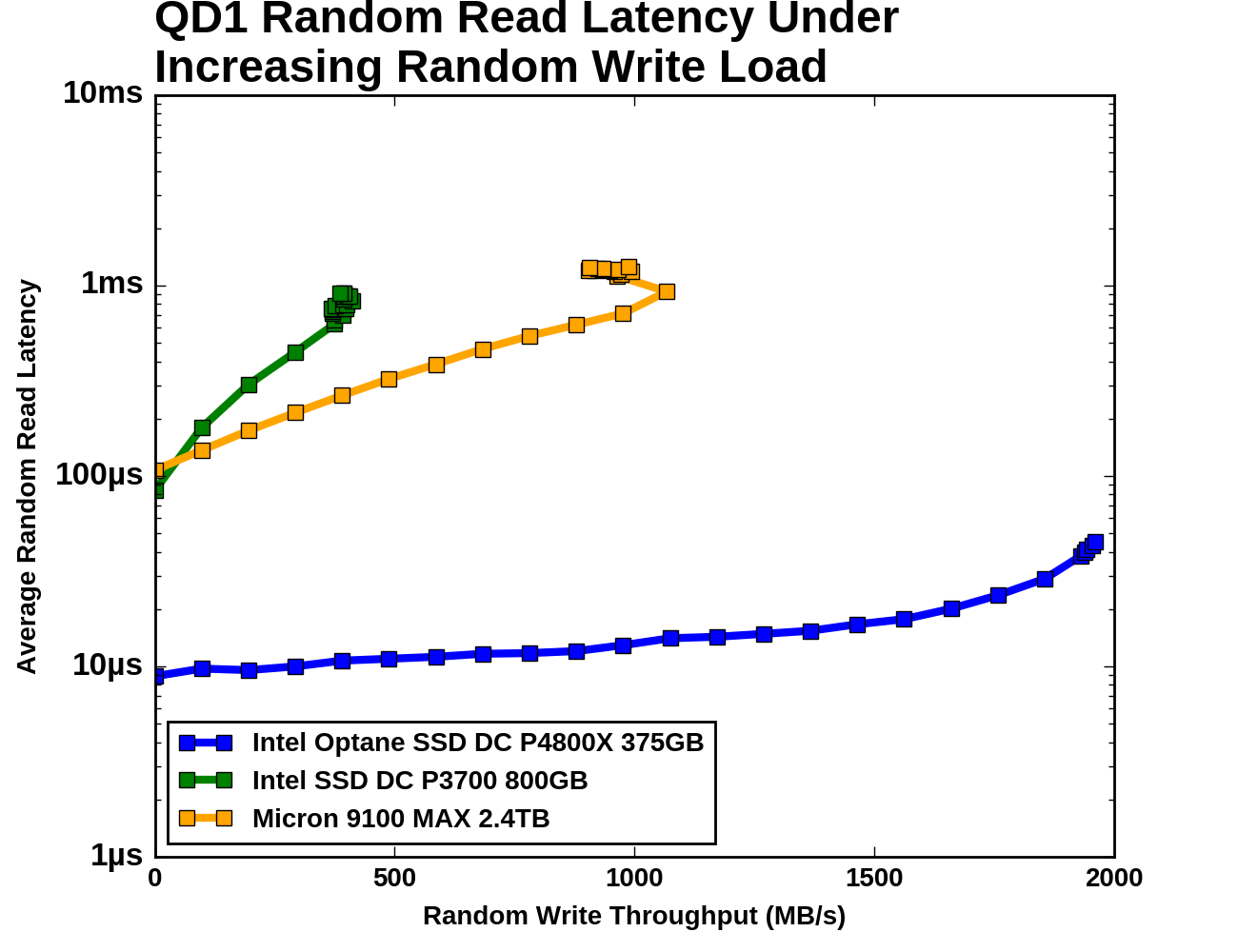
The three SSDs have very different capacity for random write throughput: the Intel P3700 tops out around 400MB/s, the Micron 9100 can sustain 1GB/s, and the Intel Optane SSD DC P4800X can sustain almost 2GB/s. The Optane SSD's average read latency increases by a factor of 5, but that still enough to provide about 25k read IOPS. The flash SSDs both experience read latency growing by an order of magnitude as write throughput approaches saturation. Even though the Intel P3700 has a much lower capacity for random writes, it provides slightly lower random read latency at its saturation point than the Micron 9100. When comparing the two flash SSDs with the same write load, the Micron 9100 provides far more random read throughput.


117 Comments
View All Comments
melgross - Tuesday, April 25, 2017 - link
You're making the mistake those who know nothing make, which is surprising for you. This is a first generation product. It will get much faster, and much cheaper as time goes on. NAND will stagnate. You also have to remember that Intel never made the claim that this was as fast as RAM, or that it would be. The closest they came was to say that this would be in between NAND and RAM in speed. And yes, for some uses, it might be able to replace RAM. But that could be several generations down the road, in possibly 5 years, or so.tuxRoller - Sunday, April 23, 2017 - link
I'm not sure i understand you.You talk about "pages", but, i hope, the reviewer was only using dio, so there would be no page cache.
It's very unclear where you are getting this "~100x" number. Nvme connected dram has a plurality of hits around 4-6 us (depending on software) but it also has a distributed latency curve. However, i don't know what the latency at the 99.999% percentile. The point is that even with dram's sub-100ns latency, it's still not staying terribly close to the theoretical min latency of the bus.
Btw, it's not just the controller. A very large amount of latency comes from the block layer itself (amongst other things).
Santoval - Tuesday, June 6, 2017 - link
It is quite possible that Intel artificially weakened P4800X's performance and durability in order to avoid internal competition with their SSD division (they already did the same with Atoms). If your new technology is *too* good it might make your other more mainstream technology look bad in comparison and you could see a big drop in sales. Or it might have a "deflationary" effect, where their customers might delay buying in hope of lower prices later. This way they can also have a more clear storage hierarchy, business segment wise, where their mainstream products are good, and their niche ones are better but not too good.I am not suggesting that it could ever compete with DRAM, just that the potential of 3D XPoint technology might actually be closer to what they mentioned a year ago than the first products they shipped.
albert89 - Friday, April 21, 2017 - link
Intel wont be reducing the price of the optane but rather will be giving the average consumer a watered down version which will be charged at a premium but perform only slightly better then the top SSD. The conclusion ? Another over priced ripoff from Intel.TheinsanegamerN - Thursday, April 20, 2017 - link
the fastest SSD on the consumer market is the 960 pro, which can hit 3.2GB/s read under certain circumstances.This is the equivalent of single channel DDR 400 from 2001. and DDR had far lower latencys to boot.
We are a long, long way from replacing RAM with storage.
ddriver - Friday, April 21, 2017 - link
What makes the most impression is it took a completely different review format to make this product look good. No doubt strictly following intel's own review guidelines. And of course, not a shred of real world application. Enter hypetane - the paper dragon.ddriver - Friday, April 21, 2017 - link
Also, bandwidth is only one side of the coin. Xpoint is 30-100+ times more latent than dram, meaning the CPU will have to wait 30-100+ times longer before it has data to compute, and dram is already too slow in this aspect, so you really don't want to go any slower.I see a niche for hypetane - ram-less systems, sporting very slow CPUs. Only a slow CPU will not be wasted on having to wait on working memory. Server CPUs don't really need to crunch that much data either, if any, which is paradoxical, seeing how intel will only enable avx512 on xeons, so it appears that the "amazingly fast" and overpriced hypetane is at home only in simple low end servers, possibly paired with them many core atom chips. Even overpriced, it will kind of a decent deal, as it offers about 3 times the capacity per dollar as dram, paired with wimpy atoms it could make for a decent simple, low cost, frequent access server.
frenchy_2001 - Friday, April 21, 2017 - link
You are missing the usefulness of it entirely.Yes, it is a niche product.
And I even agree, intel is hyping it and offering it for consumer with minimal benefit (beside intel's bottom line).
But it realistically slots between NAND and DRAM.
This review shows that it has lower latency than NAND and it has higher density than DRAM.
This is the play.
You say it cannot replace DRAM and for most usage (by far) you are true. However, for a small niche that works with very big data sets (like for finace or exploration), having more memory, although slower, will still be much faster than memory + swap (to a slower NAND storage).
Let me repeat, this is a niche product, but it has its uses.
Intel marketing is hyping it and trying to use it where its tradeoffs (particularly price) make little sense, but the technology itself is good (if limited).
wumpus - Sunday, April 23, 2017 - link
Don't be so sure that latency is keeping it from being used as [secondary] main memory. A 4GB machine can actually function (more or less) for office duty and some iffy gaming capability. I'd strongly suspect that a 4-8GB stack of HBM (preferably the low-cost 512 bit systems, as the CPU really only wants 512bit chunks of memory at a time) with the rest backed by 3dxpoint would still be effective at this high latency. Any improvement is likely to remove latency as something that would stop it (and current software can use the current stack [with PCIe connection] to work 3dxpoint as "swappable ram").The endurance may well keep this from happening (it is on par with SLC).
The other catch is that this is a pretty steep change along the entire memory system. Expect Intel to have huge internal fights as to what the memory map should look like, where the HBM goes (does Intel pay to manufacture an expensive CPU module or foist it on down the line), do you even use HBM (if Ravenridge does, I'd expect that Intel would have to if they tried to use xpoint as main memory)? The big question is what would be the "cache line" of the DRAM memory: the current stack only works with 4k, the CPU "wants" 512 bits, HBM is closer to 4k. 4k looks like a no-brainer, but you still have to put a funky L5/buffer that deals with the huge cache line or waste a ton of [top level, not sure if L3 or L4] cache by giving it 4k cache lines.
melgross - Tuesday, April 25, 2017 - link
What is it with you and RAM? This isn't a RAM replacement for most any use. Intel hasn't said that it is. Why are you insisting on comparing it to RAM?