The AMD Vega GPU Architecture Teaser: Higher IPC, Tiling, & More, Coming in H1’2017
by Ryan Smith on January 5, 2017 9:00 AM ESTFirst Thoughts: A Peek At What’s To Come
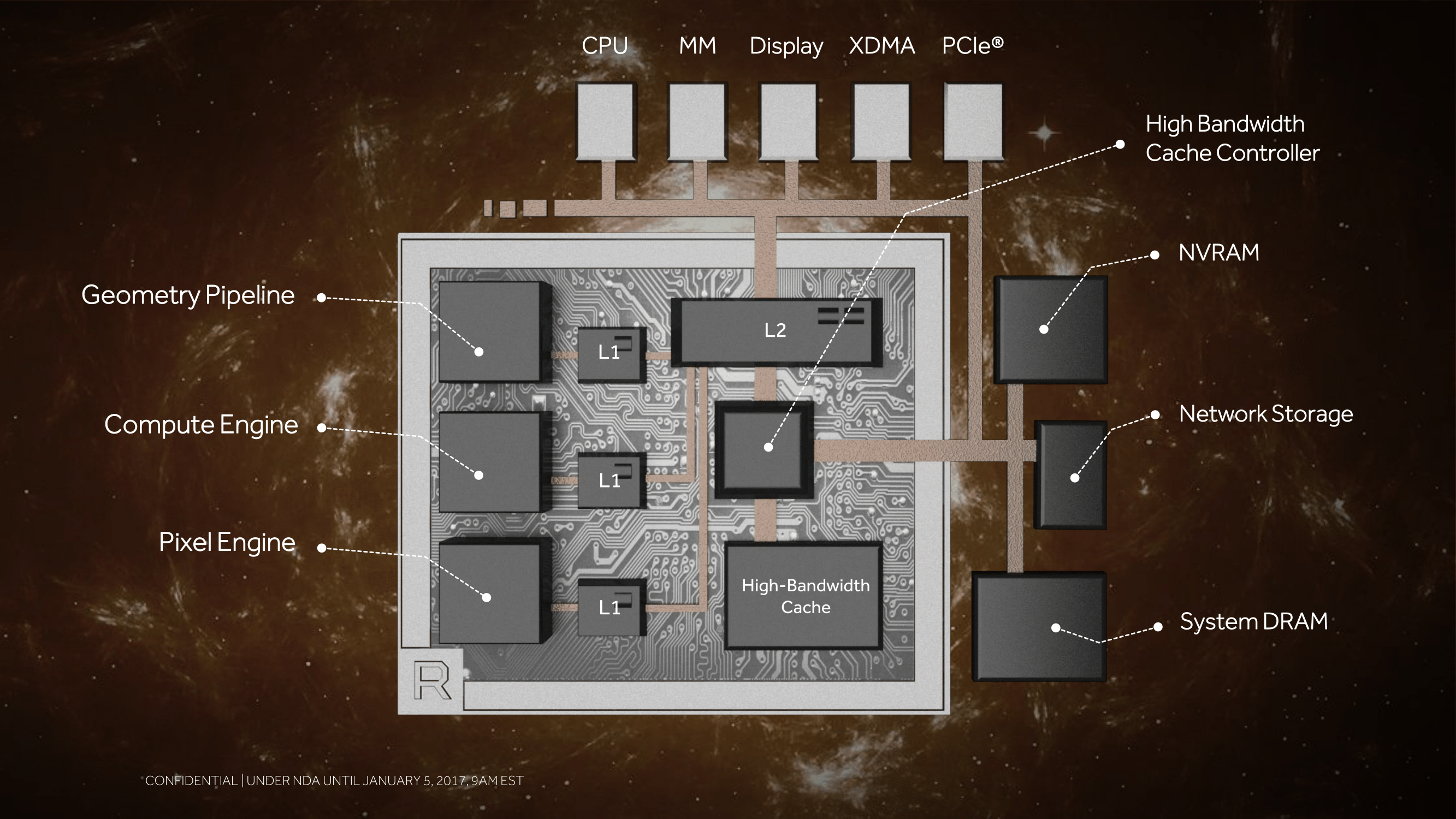
Wrapping things up, while today’s reveal from AMD is only a teaser of what they have been working on over the last few years with Vega, it’s none the less an important one. Based on what we know so far, Vega stands to be the biggest change to AMD’s GPU architecture since GCN 1.0 was released 5 years ago, and the changes to the ALUs, the ROPs, the memory structure, and other aspects of Vega reinforce this notion. To be sure, Vega is not a wholly new architecture – it is clearly a further refinement of GCN – but then this is exactly why GCN was designed to be able to evolve through refinements over a very long period of time.
What we have for now then is a quick look at what’s to come from AMD. There are still many things we don’t know, not the least of which is the actual GPU configurations. But for a teaser it’s enough to show that AMD has been hard at work. It sets the stage for the hardware and marketing ramp-up to come over the next few months.
But for now, let’s close with an image. As I mentioned before, the first Vega has taped out, and Radeon Technology Group’s frontman and Chief Architect, Raja Koduri, has one. The chip was just a few weeks old as of December, and while trying to discern die size may be a little too error-prone, we can see one important detail: 2 HBM2 packages.

Raja and AMD will not tell us what chip we’re looking at – like Polaris, two Vega chips have been confirmed – but either way we are looking at one of them in all its alpha silicon glory. Bearing in mind HBM2’s much greater bandwidth per pin, we could very well be looking at a design for a Fiji-like 512GB/sec of memory bandwidth in the chip Raja holds. And for AMD, that is one more teaser for today to keep attention focused right where they want it: on Vega ahead of its H1’17 launch.


155 Comments
View All Comments
AndrewJacksonZA - Thursday, January 5, 2017 - link
I'm kinda glad that I've procrastinated my RX480 purchase so much. Vega interests me greatly...AndrewJacksonZA - Thursday, January 5, 2017 - link
(Darn it! Where's the edit button guys?)Bring on the release date and the pricing!!! :-)
jjj - Thursday, January 5, 2017 - link
So for it looks likely that they have implemented that famous patent everybody hoped for, one way or another.Seems that higher efficiency was a focus area everywhere so they might catch up- or better?
Hard to figure out where Vega is from a perf density point of view, that matters too.
Any clue if it's on 16FF or they stick with 14nm?
If this is what it looks like, it's gonna be huge step forward and that includes APUs. Can you imagine how those APUs would perform vs the competition?
SunnyNW - Thursday, January 5, 2017 - link
I read that the die size is over 500mm2SunnyNW - Thursday, January 5, 2017 - link
Meant to add...So not sure if TSMC or GloFo but I guess it could be either since GloFo has been running their 14nm for quite a while now. I would put my money on TSMC tho because GloFo history makes me second guess them.jjj - Thursday, January 5, 2017 - link
There are perf difference between the 2 foundries, due to HBM i'm expecting TSMC but we'll see.By looking at the pic published here i would say 480mm2 but the pic is poor so the guess is likely unreliable. In any case, i am expecting it in the 400-500mm2 range.
Kepe - Thursday, January 5, 2017 - link
There's a better picture in the gallery here: https://www.io-tech.fi/uutinen/amd-esitteli-seuraa...Scroll down to the image gallery, it's the first picture.
jjj - Thursday, January 5, 2017 - link
TR has a much better one but didn't had time to try to measure it based on the HBM 2 package size http://techreport.com/r.x/amdvegapreview/vegachip....extide - Thursday, January 5, 2017 - link
HBM2 die is about ~8x12mm. So, the long (12mm) sides of the HBM die are facing the GPU die, and 2 of them are a bit shorter than the GPU die. I am going to guess that the GU die is about 25mm wide. It looks like it is a bit shorter than it is wide -- so say 20mm. 25x20mm makes a 500mm chip, That seems about right. Smaller die than Fiji, much smaller interposer because of only 2 stacks of HBM, this thing should end up costing a lot less than Fiji to produce once the volume gets ramped, and hopefully it should smoke it performance-wise as well.extide - Thursday, January 5, 2017 - link
^^ Based on this pic http://techreport.com/r.x/amdvegapreview/vegachip.... which is the most square on and clear pic I can find right now. I was initially thinking it was 400mm^2 and change, but now I am thinking it is closer to 500mm^2 and change.