The AMD Vega GPU Architecture Teaser: Higher IPC, Tiling, & More, Coming in H1’2017
by Ryan Smith on January 5, 2017 9:00 AM ESTHBM2 & “The World’s Most Scalable GPU Memory Architecture”
With the launch of the Fiji GPU and resulting Radeon R9 Fury products in 2015, AMD became the first GPU manufacturer to ship with first-generation High Bandwidth Memory (HBM). The ultra-wide memory standard essentially turned the usual rules of GPU memory on its head, replacing narrow, high clocked memory (GDDR5) with wide, low clocked memory. By taking advantage of Through Silicon Vias (TSVs) and silicon interposers, HBM could offer far more bandwidth than GDDR5 while consuming less power and taking up less space.
Now for Vega, AMD is back again with support for the next generation of HBM technology, HBM2. In fact this is the very first thing we ever learned about Vega, going back to AMD’s roadmap from last year where it was the sole detail listed for the architecture.
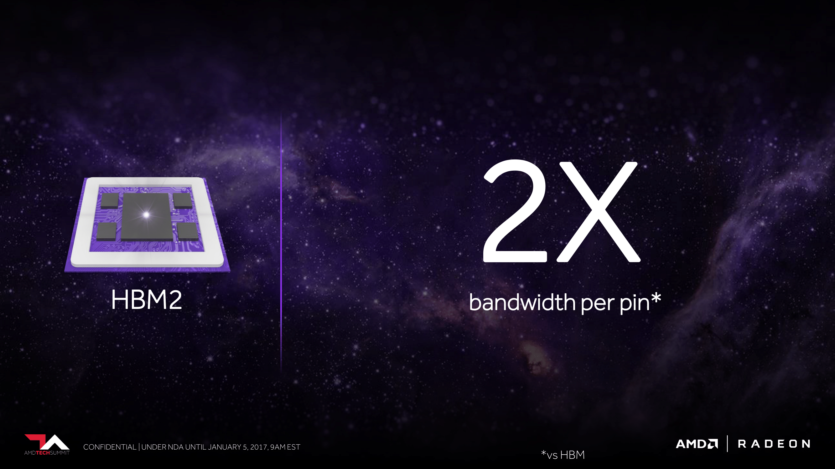
HBM2 builds off of HBM, offering welcome improvements in both bandwidth and capacity. In terms of bandwidth, HBM2 can clock at up to 2Gbps per pin, twice the rate of HBM1. This means that at those clockspeeds (and I’ll note that at least so far we haven’t seen any 2Gbps HBM2), AMD can either double their memory bandwidth or cut the number of HBM stacks they need in half to get the same amount of bandwidth. The latter point is of particular interest, as we’ll get to here in a bit.
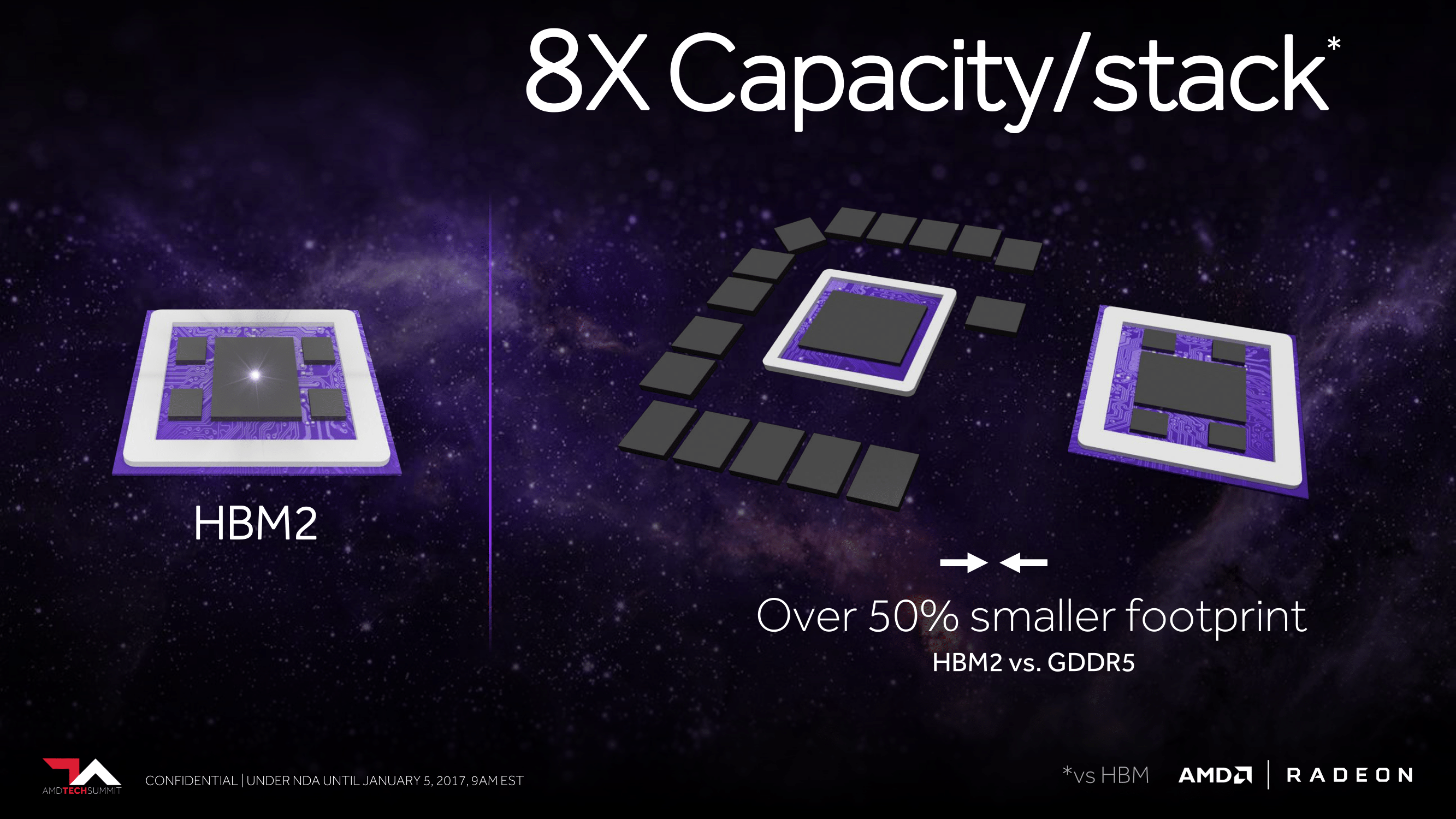
But more important still are the capacity increases. HBM1 stacked topped out at 1GB each, which means Fiji could have no more than 4GB of VRAM. HBM2 stacks go much higher – up to 8GB per stack – which means AMD’s memory capacity problems when using HBM have for all practical purposes gone away. AMD could in time offer 8GB, 16GB, or even 32GB of HBM2 memory, which is more than competitive with current GDDR5 memory types.
Meanwhile it’s very interesting to note that with Vega, AMD is calling their on-package HBM stacks “high-bandwidth cache” rather than “VRAM” or similar terms as was the case with Fiji products.
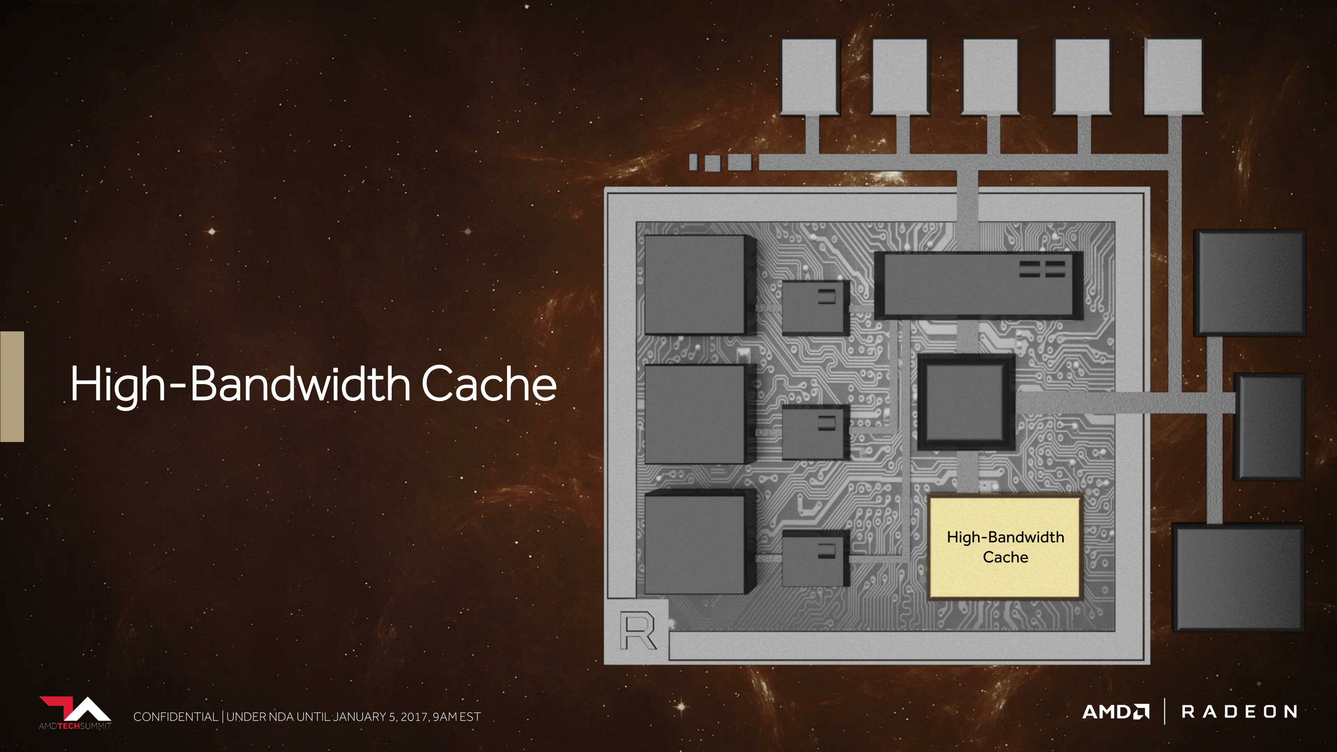
This is a term that can easily be misread – and it’s the one area where perhaps it’s too much of a tease – but despite the name, there are no signals from AMD right now that it’s going to be used as a cache in the pure, traditional sense. Rather, because AMD has already announced that they’re looking into other ideas such as on-card NAND storage (the Radeon Pro SSG), they are looking at memory more broadly.
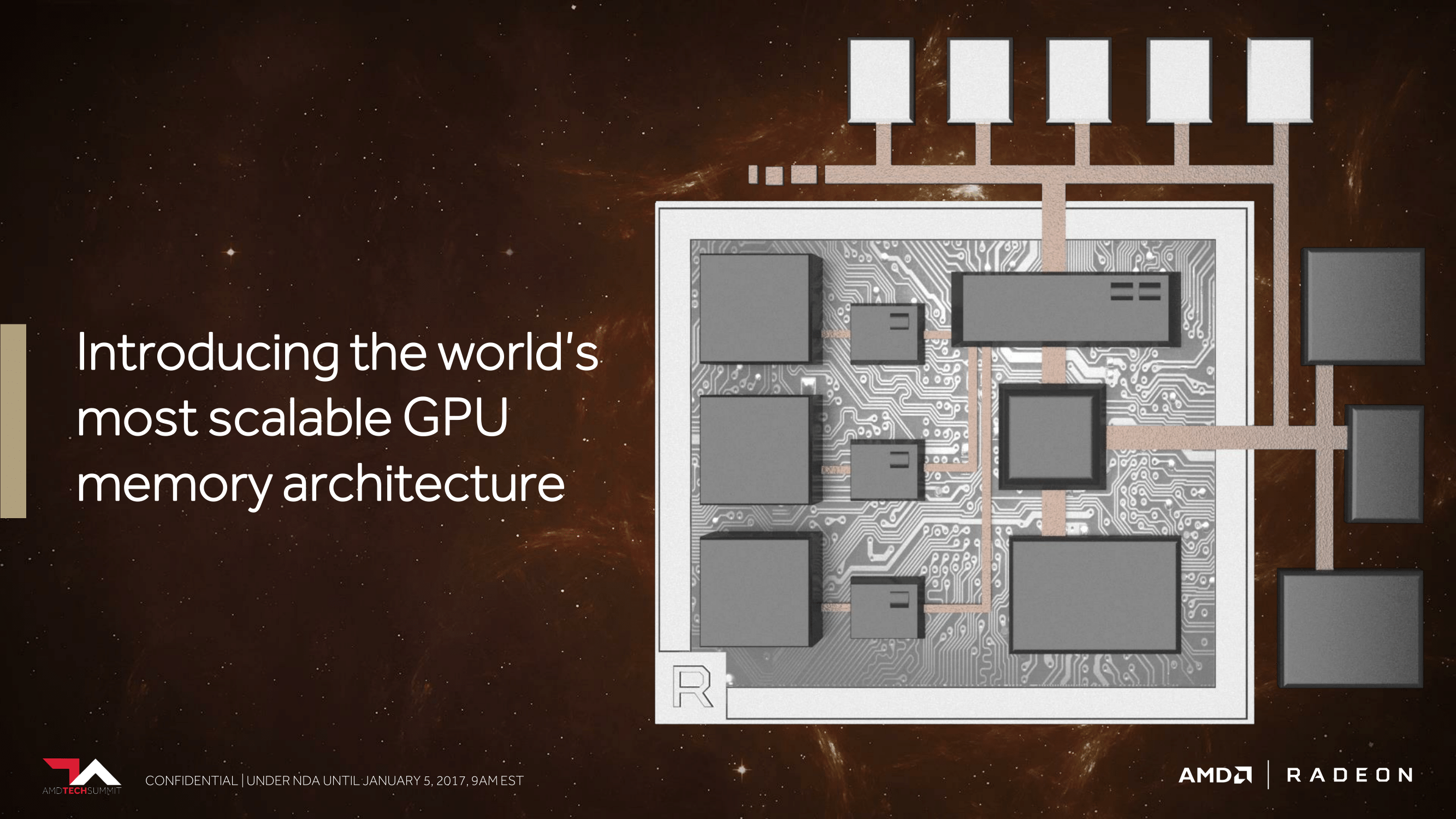
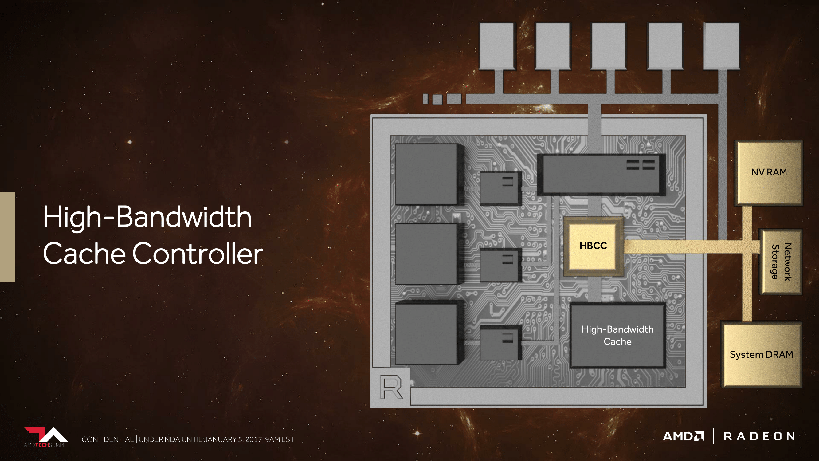
And this brings us to what AMD is calling “The World’s Most Scalable GPU Memory Architecture”. Along with supporting HBM, AMD has undertaken a lot of under-the-hood work to better support large dataset management between the high bandwidth cache (HBM2), on-card NAND, and even farther out sources like system RAM and network storage.
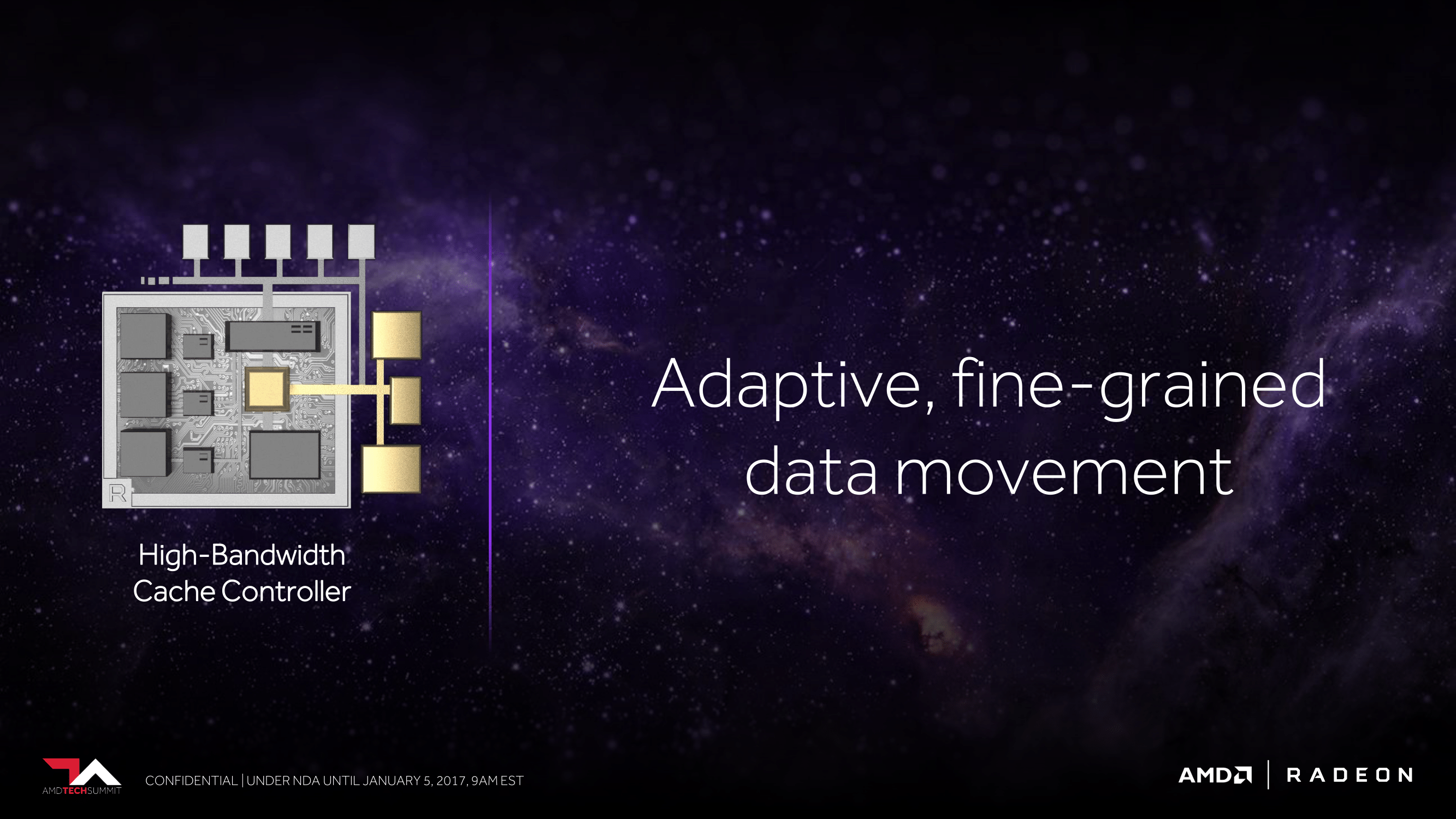
The basic idea here is that, especially in the professional space, data set size is vastly larger than local storage. So there needs to be a sensible system in place to move that data across various tiers of storage. This may sound like a simple concept, but in fact GPUs do a pretty bad job altogether of handling situations in which a memory request has to go off-package. AMD wants to do a better job here, both in deciding what data needs to actually be on-package, but also in breaking up those requests so that “data management” isn’t just moving around a few very large chunks of data. The latter makes for an especially interesting point, as it could potentially lead to a far more CPU-like process for managing memory, with a focus on pages instead of datasets.
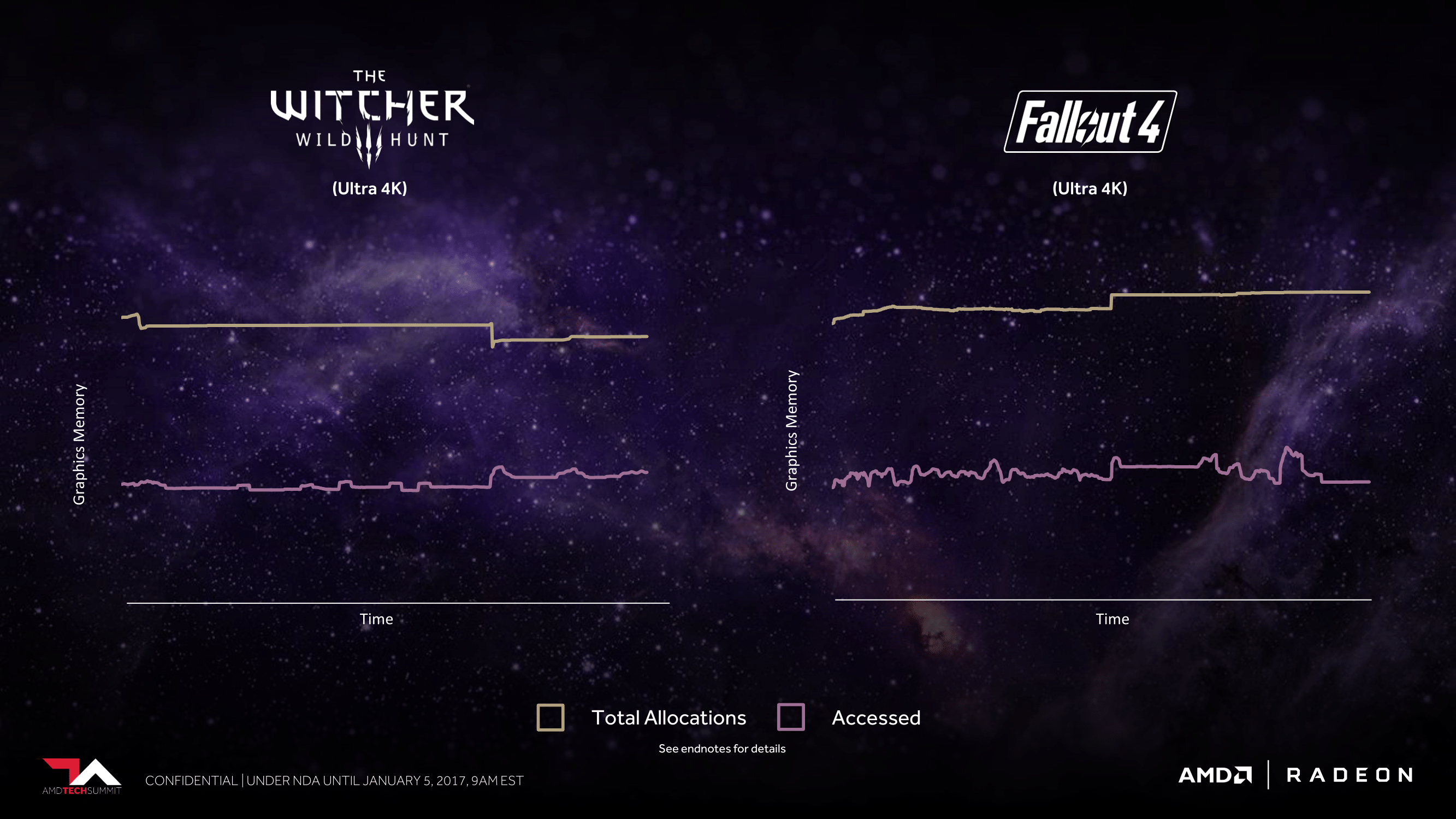
Interestingly, to drive this point home, AMD actually turned to games rather than professional applications. Plotting out the memory allocation and usage patterns of The Witcher III and Fallout 4, AMD finds that both games allocate far more memory than they actually use, by nearly a factor of 2x. Part of this is undoubtedly due to the memory management model of the DirectX 11 API used by both games, but a large factor is also simply due to the fact that this is traditionally what games have always done. Memory stalls are expensive and games tend to be monolithic use cases, so why not allocate everything you can, just to be sure you don’t run out?
The end result here is that AMD is painting a very different picture for how they want to handle memory allocations and caching on Vega and beyond. In the short term it’s professional workloads that stand to gain the most, but in the long run this is something that could impact games as well. And not to be ignored is virtualization; AMD’s foray into GPU virtualization is still into its early days, but this likely will have a big impact on virtualization as well. In fact I imagine it’s a big reason why AMD is giving Vega the ability to support a relatively absurd 512TB of virtual address space, many times the size of local VRAM. Multi-user time-sharing workloads are a prime example of where large address spaces can be useful.
ROPs & Rasterizers: Binning for the Win(ning)
We’ll suitably round-out our overview of AMD’s Vega teaser with a look at the front and back-ends of the GPU architecture. While AMD has clearly put quite a bit of effort into the shader core, shader engines, and memory, they have not ignored the rasterizers at the front-end or the ROPs at the back-end. In fact this could be one of the most important changes to the architecture from an efficiency standpoint.
Back in August, our pal David Kanter discovered one of the important ingredients of the secret sauce that is NVIDIA’s efficiency optimizations. As it turns out, NVIDIA has been doing tile based rasterization and binning since Maxwell, and that this was likely one of the big reasons Maxwell’s efficiency increased by so much. Though NVIDIA still refuses to comment on the matter, from what we can ascertain, breaking up a scene into tiles has allowed NVIDIA to keep a lot more traffic on-chip, which saves memory bandwidth, but also cuts down on very expensive accesses to VRAM.
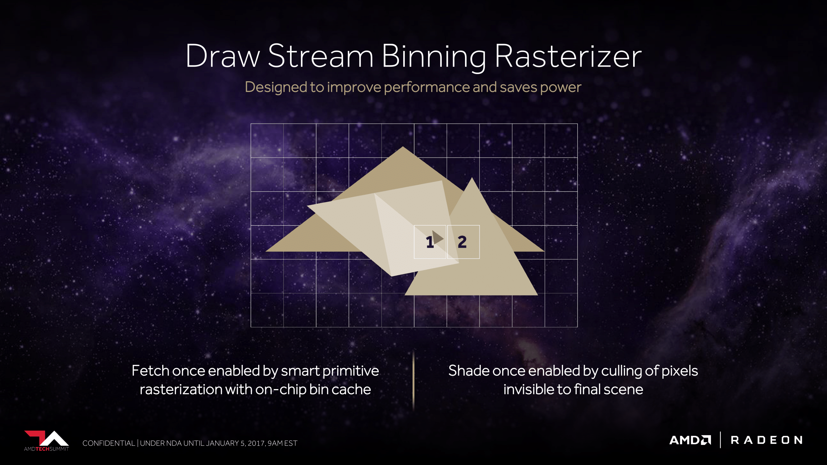
For Vega, AMD will be doing something similar. The architecture will add support for what AMD calls the Draw Stream Binning Rasterizer, which true to its name, will give Vega the ability to bin polygons by tile. By doing so, AMD will cut down on the amount of memory accesses by working with smaller tiles that can stay-on chip. This will also allow AMD to do a better job of culling hidden pixels, keeping them from making it to the pixel shaders and consuming resources there.
As we have almost no detail on how AMD or NVIDIA are doing tiling and binning, it’s impossible to say with any degree of certainty just how close their implementations are, so I’ll refrain from any speculation on which might be better. But I’m not going to be too surprised if in the future we find out both implementations are quite similar. The important thing to take away from this right now is that AMD is following a very similar path to where we think NVIDIA captured some of their greatest efficiency gains on Maxwell, and that in turn bodes well for Vega.
Meanwhile, on the ROP side of matters, besides baking in the necessary support for the aforementioned binning technology, AMD is also making one other change to cut down on the amount of data that has to go off-chip to VRAM. AMD has significantly reworked how the ROPs (or as they like to call them, the Render Back-Ends) interact with their L2 cache. Starting with Vega, the ROPs are now clients of the L2 cache rather than the memory controller, allowing them to better and more directly use the relatively spacious L2 cache.

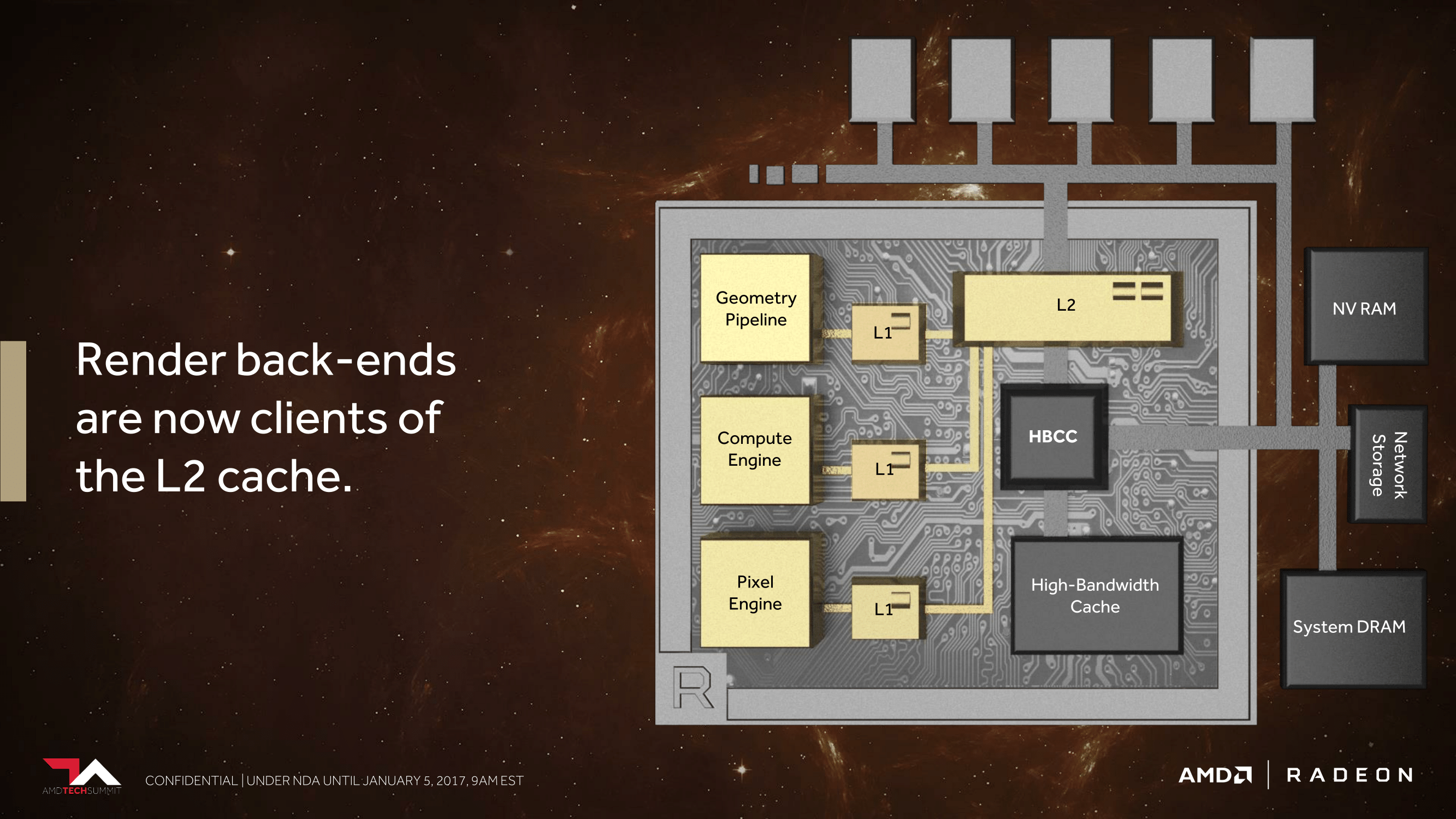
This is especially significant for a specific graphics task, which is rendering to a texture (as opposed to a frame buffer to be immediately displayed). Render to texture is an especially common operation for deferred shading, and while deferred shading itself isn’t new, its usage is increasing. With this change to Vega, the ROPs can now send a scene rendered to a texture to the L2 cache, which can in turn be fetched by the texture units for reuse in the next stage of the rendering process. Any potential performance improvements from this change are going to be especially game-specific since not every game uses deferred shading, but it’s one of those corner cases that is important for AMD to address in order to ensure more consistent performance.


155 Comments
View All Comments
jjj - Thursday, January 5, 2017 - link
I get to some 500mm2 too.As for cost, Fiji was on 28nm, much cheaper on an area basis. They will get better yield for packaging but the overall costs will be much higher than with Fiji. They could have a SKU with 25% of the CUs disabled at 499$ and the full Vega 10 at 699 to .. the upper limit depends on where perf lands vs Titan X.
Yojimbo - Friday, January 6, 2017 - link
One must also consider the difference in cost of the process that each chip is made with as well as the price of the larger capacity of HBM2 compared to smaller amount of HBM1. But a smaller interposer will definitely help.It'd better smoke Fiji performance-wise. I think it's a foregone conclusion that it will, though. Judging by their released benchmarks I'm guessing it'll be modestly faster than the 1080, on average, but significantly slower than a forthcoming 1080Ti. So it'll probably be priced around the same $650 as the Fury X.
jjj - Friday, January 6, 2017 - link
You are rushing into judging perf in a big way.AMD is demoing Vega, just showing it up and running ,NOT showing perf. Not quite sure why so many don't get that.
You can bet that it is using early software and that it's clocked at 1-1.2GHz only for now.They are not gonna show their hand ,months before retail availability. They are just showing 4k gaming at 60FPS or better.
You can look at min perf Vega 10 should offer in many ways.
1. It is assumed to have same number of "cores" as the Fury X but almost 50% higher clocks. Then,some 15% architectural and software gains would put it on par with Titan X. So the question is, if they can do better and by how much and at what power.
A note here, given the number of cores , the scaling from 28nm to 14/16nm is very poor. They are clearly sacrificing area for huge gains elsewhere, you wouldn't do it otherwise. 16 and 8 bit is on thing but there must be a lot more.
2. Even the Polaris architecture scaled to 12.5TFLOPS and this memory bandwidth, would match the Titan X. So the question is, how much better can they do.
One could argue that AMD is nuts and Vega is worse than Polaris but that's less than reasonable.
eachus - Saturday, January 14, 2017 - link
The 12.5 TFLOPS is Vega 10 doing 16-bit floating point, not Polaris. And this, in part, explains why Vega 10 doesn't scale well compared to Fury X. There is a new compute engine with lots of new features. I'm hoping that one of them is a fused multiply-add, but we do know that it can do 16-bit floating point twice as fast as single precision (32 bit).So remember that, for now, any comparisons you see with Vega will almost certainly use none of the new features. AMD can and should spend most of their driver effort right now on changes that benefit Polaris. Some support for Vega? Sure, but don't expect support for the new features in drivers until just before (or after) Vega ships.
SunnyNW - Thursday, January 5, 2017 - link
With AMD's countdown on the ve.ga site and their marketing almost everyone thought their would be a live stream incoming, but instead it was a countdown to an NDA lift, like really AMD? I believe AMD made a huge mistake here because there are A LOT of angry people out there whom were waiting with much anticipation. I kinda thought something was odd with the time being 6 a.m. PST and had told my friends as much but still they were convinced too that it was for a live stream.Why has AMD marketing been SO bad for so long, I do think they have gotten a little better in recent history but they are way behind Nvidia for example. It's like AMD has kept the same marketing team for years and years and just does not want to let them go for who knows what reason. In business when you fail for so long who are usually replaced, has AMD just been replacing under-performer after another or just keeping the same people I just don't get it.
And this is coming from someone who is an AMD supporter and would like to see them succeed.
Michael Bay - Thursday, January 5, 2017 - link
Marketing is where careers go to die. If you can even call those things careers.What else do you expect?
alphasquadron - Thursday, January 5, 2017 - link
Marketing for large companies is usually one of the higher paid positions. The ability to persuade a mass of people gets you paid well.eldakka - Friday, January 6, 2017 - link
like a cult leader?The_Assimilator - Friday, January 6, 2017 - link
This is exactly my biggest problem with AMDL: their marketing is, to be frank, absolute bullshit. It's why I don't trust them to deliver on their promises until I see independent reviewers validate them, while if Intel says their next chip is going to have an extra 10% IPC or NVIDIA says their next GPU is going to be 20% faster, I'm inclined to believe those companies.AMD marketing needs to understand the difference between hype and lies, and that consistent lies hurt them far more than they help.
Meteor2 - Friday, January 6, 2017 - link
This. I'm tiring of AMD 'teasing' products.When will it be available? What can it do? How much will it cost? This is what I want to know.