Intel Announces 7th Gen Kaby Lake: 14nm PLUS, Six Notebook SKUs, Desktop coming in January
by Ganesh T S & Ian Cutress on August 30, 2016 9:00 AM EST- Posted in
- CPUs
- Intel
- 14nm
- Kaby Lake
- Gen 9
- Speed Shift
- Turbo Boost
A New Optimized 14nm Process: 14nm+
One of the mysteries with the launch of Kaby Lake is the optimized 14nm+ process that Intel is promoting as one of the key components for the performance uptick in Kaby Lake. It’s worth noting that Intel has said nothing about caches, latencies or bandwidths. We are being told that the underlying microarchitecture for Kaby Lake is the same as Skylake, and that the frequency adjustments from the new process, along with features such as Speed Shift v2 and the new fixed function media codecs, account for the performance improvements as well as battery life increases when dealing with 4K content.
For users that speak in pure IPC, this may/may not be a shock. Without further detail, Intel is implying that Kaby Lake will have the same IPC as Skylake, however it will operate with a better power efficiency (same frequency at lower power, or higher frequency at same power) and for media consumption there will be more idle CPU cycles with lower power drain. The latter makes sense for mobile devices such as tablets, 2-in-1s and notebooks, or for power conscious users, but paints a static picture for the future of the desktop platform in January if the user only gets another 200-400 MHz in base frequencies.
However I digress with conjecture – the story not being told is on how has Intel changed its 14nm+ platform. We’ve only been given two pieces of information: taller fins and a wider gate pitch.
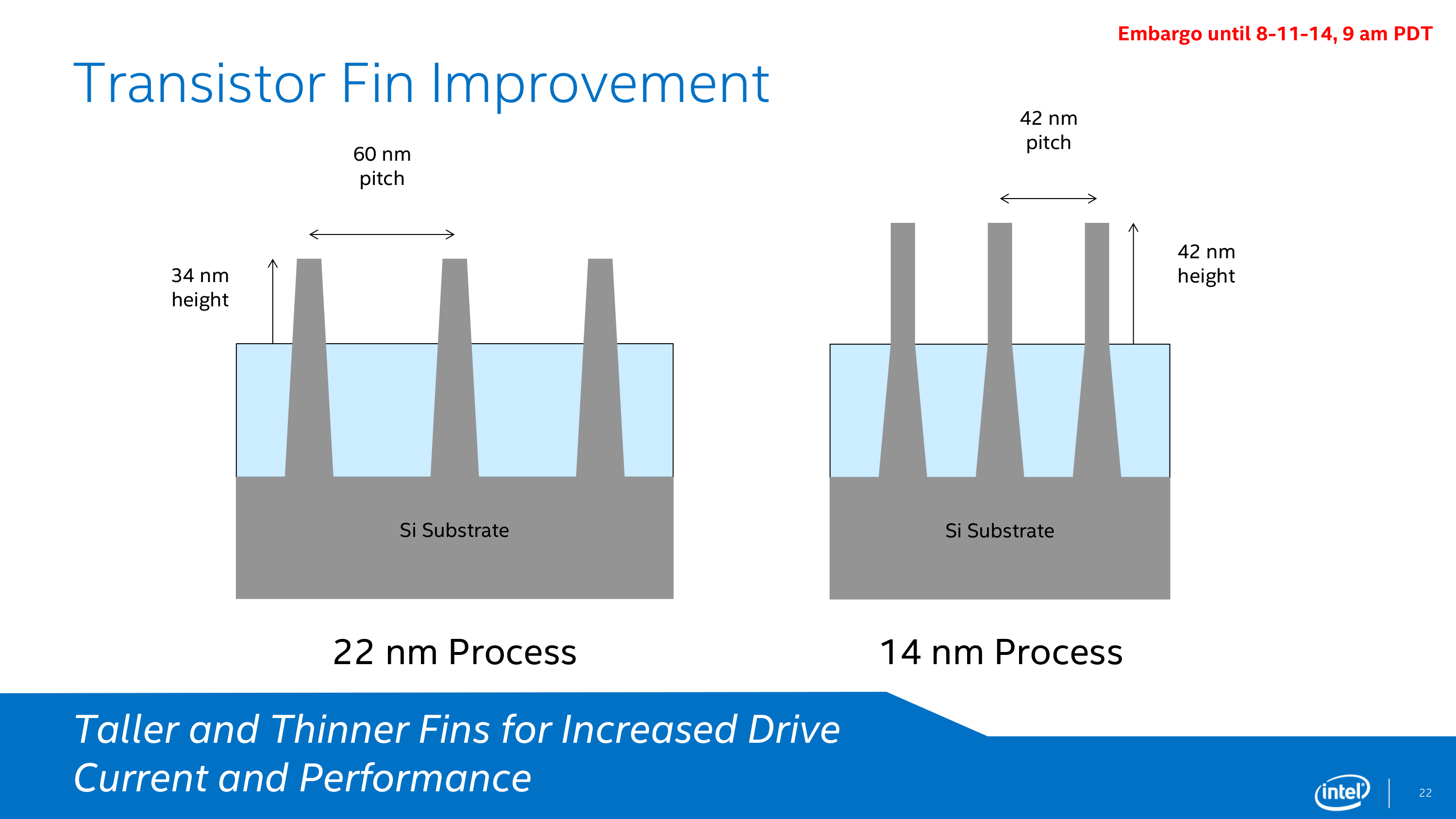
Intel 14nm Circa Broadwell
When Intel launched Broadwell on 14nm, we were given an expose into Intel’s latest and greatest semiconductor manufacturing lithography node. Intel at its core is a manufacturing company rather than a processor company, and by developing a mature and robust process node allows them to gain performance advantages over the other big players: TSMC, Samsung and GlobalFoundries. When 14nm was launched, we had details on their next generation of FinFET technology, discussions about the issues that faced 14nm as it was being developed, and fundamental dimensional data on how transistors/gates were proportioned. Something at the back of my brain says we’ll get something similar for 10nm when we are closer to launch.
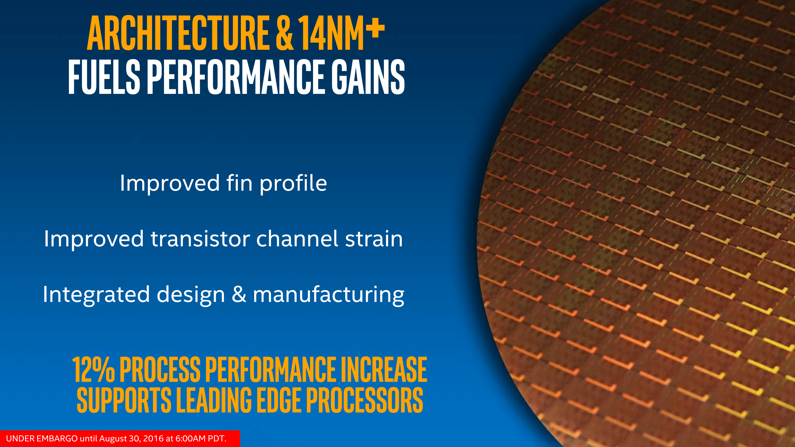
But as expected, 14nm+ was given little extra detail. What would interest me is the scale of results or problems faced by the two changes in the process we know about. Taller fins means less driving current is needed and leakage becomes less of an issue, however a wider gate pitch is typically associated with a decrease in transistor density, requiring higher voltages but making the manufacturing process easier. There is also the argument that a wider pitch allows the heat generation of each transistor to spread more before affecting others, allowing a bit more wiggle room for frequency – this is at least how Intel puts it.
The combination of the two allows for more voltage range and higher frequencies, although it may come at the expense of die size. We are told that transistor density has not changed, but unless there’s a lot of spare unused silicon in the die for the wider pitch to spread, it seems questionable. It also depends which part of the metal stack is being adjusted as well. It’s worth noting that Intel has not released die size information at this time (we may get more exact numbers in January), and transistor counts as a metric is not being disclosed, similar to Skylake.
Finally, there's some question over what it takes at a fab level to produce 14nm+. Though certainly not on the scale of making the jump to 14nm to begin with, Intel has been tight-lipped on whether any retooling is required. At a minimum, as this is a new process (in terms of design specificaitons), I think it's reasonable to expect that some minor retooling is required to move a line over to 14nm+. In which case the question is raised over which Intel fabs can currently produce chips on the new process. One of the D1 fabs in Oregon is virtually guaranteed; whether Arizona or Ireland is also among these is not.
I bring this up because of the parallels between the Broadwell and Kaby Lake launches. Both are bottom-up launches, starting with the low wattage processors. In Broadwell's case, 14nm yields - and consequently total volume - were a bottleneck to start with. Depending on the amount of retooling required and which fabs have been upgraded, I'm wondering whether the bottom-up launch of Kaby Lake is for similar reasons. Intel's yields should be great even with a retooling, but if it's just a D1 fab producing 14nm+, then it could be that Intel is volume constrained at launch and wants to focus on producing a larger number of small die 2+2 processors to start with, ramping up for larger dies like 4+2 and 4+4e later on.
Speed Shift v2
One of the new features for Skylake was Speed Shift. With the right OS driver, the system could relinquish control of CPU turbo to the CPU itself. Using internal metric collection combined with access to system-level sensors, the CPU could adjust the frequency with more granularity and faster than the OS can. The purpose of Speed Shift was to allow the system to respond quicker to requests for performance (such as interacting with a touch screen or browsing the web), reduce delays and improve the user experience. So while the OS was limited to predefined P-state options, a Speed Shift enabled processor with the right driver had a near contiguous selection of CPU multipliers within a wide range to select from.
The first iteration of Speed Shift reduced the time for the CPU to hit peak frequencies from ~100 milliseconds down to around 30. The only limitation was the OS driver, which is now a part of Windows 10 and comes by default. We extensively tested the effects of the first iteration of Speed Shift at launch.
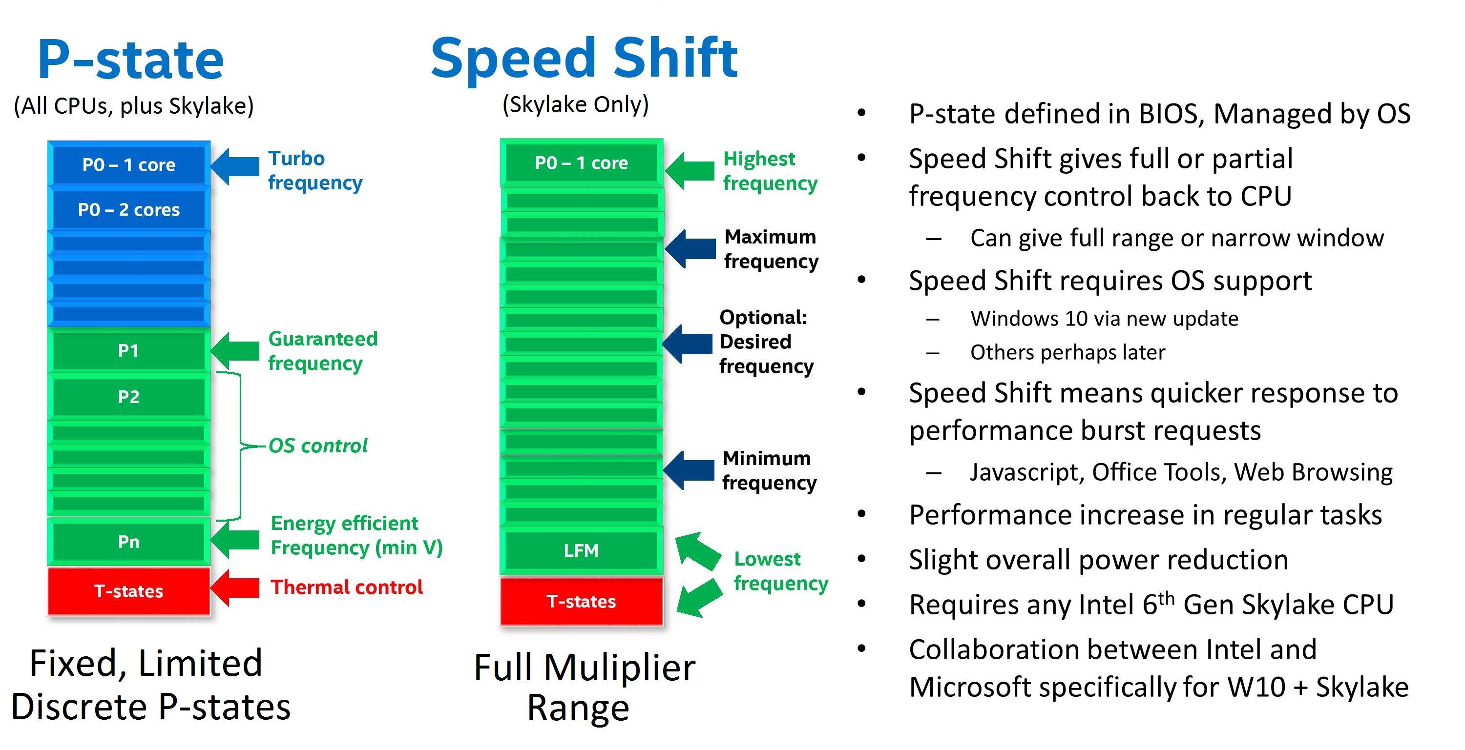
With Skylake, the hardware control around Speed Shift has improved. Intel isn’t technically giving this a new name, but it is an iterative updated which I prefer to call ‘v2’, if only because the adjustment from v1 to v2 is big enough to note. There is no change in the OS driver, so the same Speed Shift driver works for both v1 and v2, but the performance means that a CPU can now reach peak frequency in 10-15 milliseconds rather than 30.
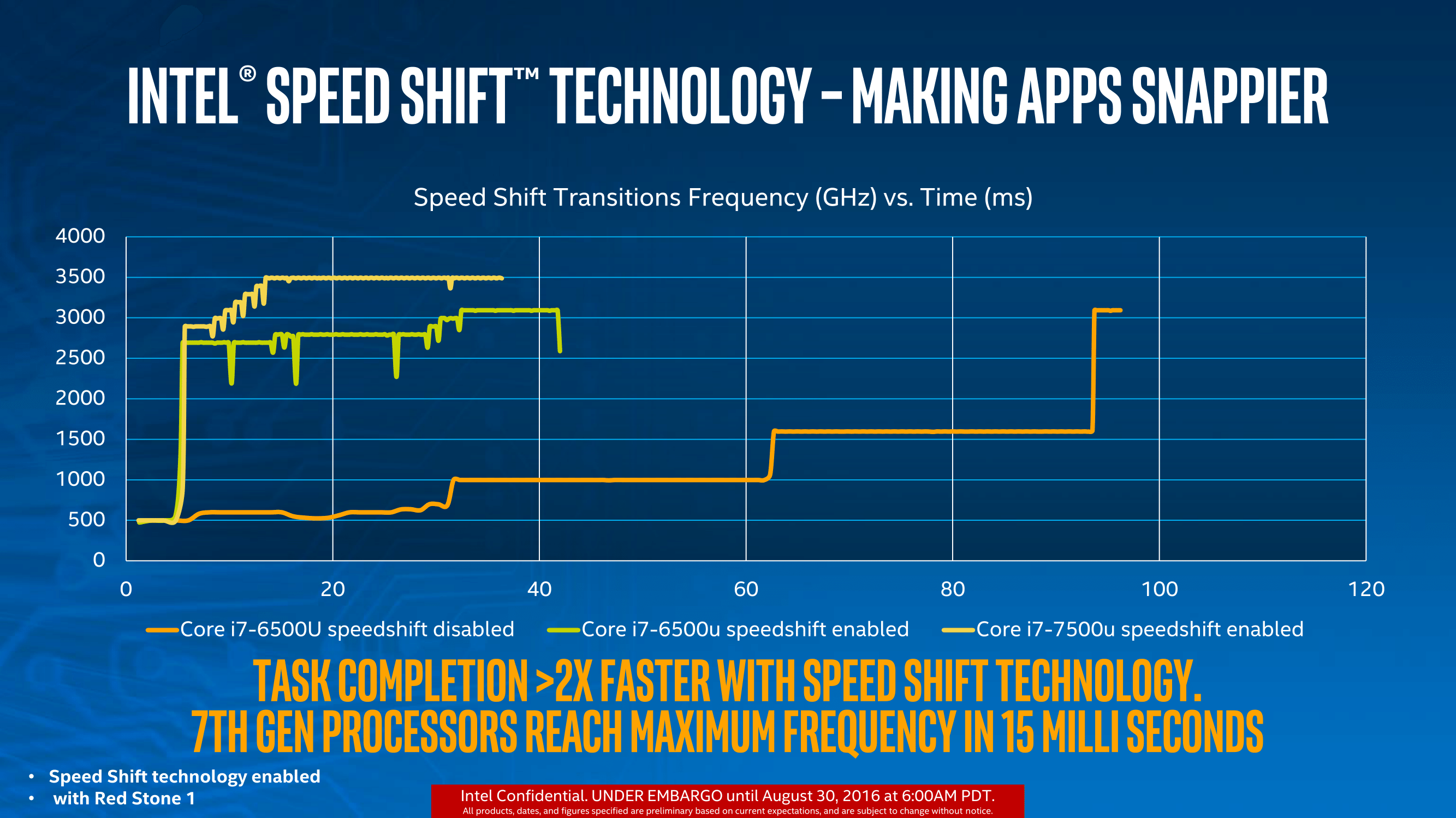
The green and yellow lines show the difference between v1 and v2, with the Core i7-7500U getting up to 3.5 GHz incredibly quickly. This will have an impact on latency limited interactions as well as situations where delays occur, such as asynchronous web page loading. Speed Shift is a play for user experience, so I’m glad to see it is being worked on. We will obviously have to test this when we can.
A note about the graph, to explain why the lines seem to zig-zag between lower and higher frequencies because I have encountered this issue in the past. Intel’s test, as far as we were told, relies on detecting register counters that increment as instructions are processed. By monitoring the value of these registers, the frequency can be extrapolated. Depending on the polling time, or adjacent point average (a common issue with counter based time benchmarks I’ve experienced academically), it can result it statistical variation depending on the capability of the code.
Performance
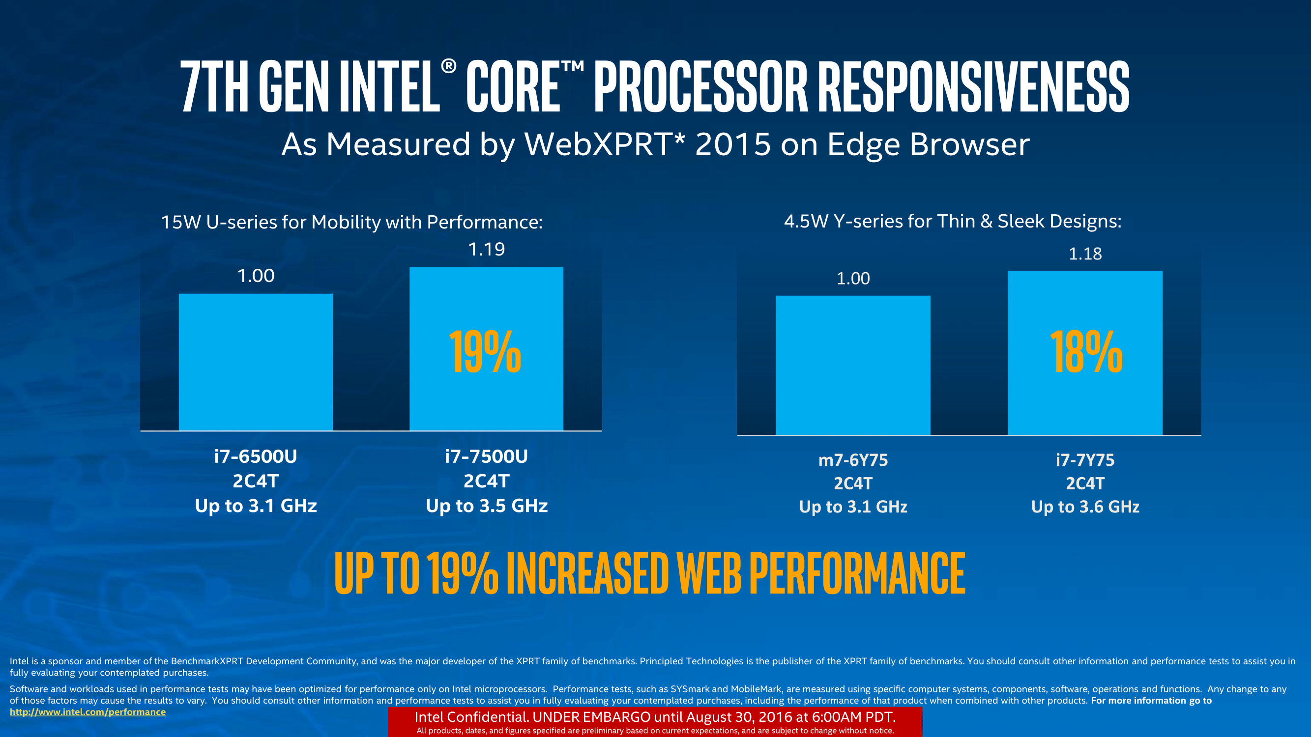
Similar to other performance claims made in the past couple of weeks, Intel was keen to show off how their new processors beat their old processors, as well as step over and above the really old stuff. Of course, benchmarks were selected that align with Intel’s regular development community, but Intel is claiming a 19% improvement in web performance over the previous generation:
Or a 12% performance uplift in general productivity taking into account various media/processing/data workloads provided by SYSMark:

For pure frequency adjustments, +400 MHz on 3.1 GHz is a 12.9% improvement, whereas +500 MHz on 3.1 GHz is a 16.1%. This accounts for most of the performance improvements for these tests, with WebXPRT extensively relying on short bursts of work to take advantage of Speed Shift v2 (WebXPRT was also a premium candidate for v1).
Perhaps a more important metric for improvement is how Intel has tackled 4K with their fixed function hardware. Moving the ability to encode/decode video from generic all-purpose hardware to fixed function allows the device to save CPU cycles but also save significant power. On a mobile device geared to consuming content, this translates as a direct improvement in battery life, assuming the display doesn’t decide to consume the excess. As we move to more efficient SoCs for video, but higher resolution displays, as long as the fixed function hardware keeps up with the content then the emphasis on battery life returns time and again to display efficiency.
With that said, Intel provided two internal metrics for power consumption when consuming 4K video in 10-bit HEVC and 8-bit VP9.
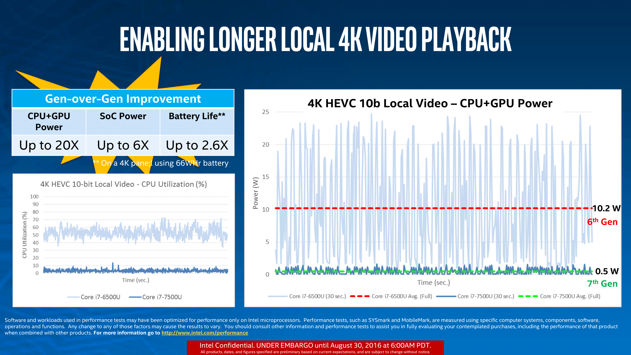
The key points for 10-bit HEVC at 4K are that CPU utilization is down to sub-5%, and system power consumption is reduced by a factor x20. Intel states that when using a 4K panel with a 66 Wh device, this translates into a 2.6x battery life improvement, or the ability to watch two films with ease.
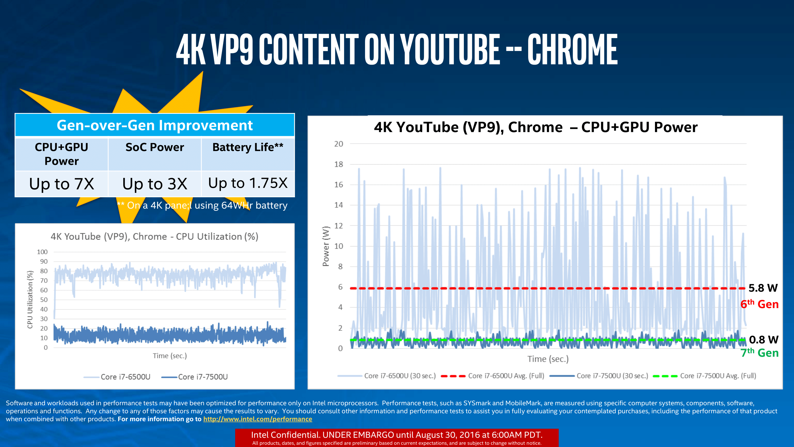
Using VP9 is YouTube’s bread and butter, with more and more YouTube content being consumed every quarter. Depending on how your browser or settings forces which codec is played, with VP9 Intel states that CPU utilization reduces from 75-80% on the SKL-U part to under 20% on the KBL-U part. Again, this was tested by Intel as a 1.75x increase in battery life. One could argue that the prevalence of 4K recording hardware (smartphones) will make this important with more users creating content for many others to consume. However it should be noted that these improvements come when the integrated graphics are used – I’m sure we will see hardware with discrete graphics in play and it will be up to the firmware to decide to use either the new fixed function parts or to engage the discrete card.
Takeaway Performance Message
On the whole, Kaby Lake comes with the following performance breakdown:
- Same IPC as Skylake, but better manufacturing gives 12-16% more frequency
- Speed Shift v2 will improve latency focused metrics, such as user experience
- New fixed function hardware for 4K HEVC/VP9 increases battery life for media consumption
- OPI 3.0 enables support for PCIe 3.0 x4 NVMe drives and Thunderbolt 3 (with additional controllers)
- Support for three 4K displays: DP 1.2, HDMI 1.4, eDP 1.2


129 Comments
View All Comments
Meteor2 - Wednesday, August 31, 2016 - link
D'oh, Apollo Lake, not Broxton.ianmills - Tuesday, August 30, 2016 - link
It is interesting that the desktop cpu will be released at the same time as zen. Maybe they think zen might be competitive and are waiting to set the final clocks once zen performance is known?CaedenV - Tuesday, August 30, 2016 - link
More likely Intel has been afraid to release anything that would put AMD out of business entirely... but at the same time they are not about to let them have a foothold on the market ever again.witeken - Tuesday, August 30, 2016 - link
Here is a more up to date graph of Intel's 14nm yield than the one shown on page 1: http://www.fudzilla.com/images/stories/2016/Januar...As you can see, Intel didn't meet its forecast of the AnandTech graph. They were quite close in H2'14, but then the yield learning slowed down considerably. In the image of AT, they forecasted parity in H1'15, but in their latest graph (mine is from november '15), they forecasted mid-2016 for yield parity compared to 22nm. My guess from what I've heard from them is that this is fairly accurate. Yields should be pretty healthy by now.
lilmoe - Tuesday, August 30, 2016 - link
Ridiculous MSRPs as usual.rahvin - Tuesday, August 30, 2016 - link
As always, but I would consider the lack of built-in USB 3.1 a stunning failure. KL was under design when the 3.1 standard was finalized. Mark my words, but this time next year every single phone tablet is going to be using Type-C. Though you can use the port without the 3.1 spec it's a stunning failure on Intel's part to not integrate it when they are a key member of the USB forum.Personally I think they are doing it because they try to push people to thunderbird but it makes their default product a failure that needs another chip to provide what will be default functionality in 12 months.
beginner99 - Wednesday, August 31, 2016 - link
USB-C and USB 3.1 are not the same thing. You can use C-connector with USB 3.0 or old connector with USB 3.1doggface - Wednesday, August 31, 2016 - link
They could have supported USB3.1, but it is a bandwidth hungry monster that takes up die space. Instead they support pcie3x4 and oems can get/pay for the extra USB3.1 chip out of their own moneys. USB-c on the other hand can be hung of pretty much anything because it is just a connector.someonesomewherelse - Thursday, September 1, 2016 - link
The only way you can expect lower prices/better chips on desktop (i3 becoming 4c/8t, i5 8c/16t, i7 12c/24t and the no gpu chip with extra cores/cache desired by pc enthusiasts (lets name it i8 and give it 18c/36t and as much extra l3 cache you can fit on it with the space gained by the removal of the gpu... you could even have i6 (14c/28t) and i4 (6c/12t) chips using the same chips with defects on some of the cores/l3 and an i2 with 3c/6t or 4c/8t but with an extremely high clock rate (5GHz+ base)), no more random removal of some instructions (K class missing some of the virtualization for example), a turbo only limited by actual heat and power, mandatory ecc, 4 channel memory (which means that the high end now gets 8 channels), extra pcie lanes, unlocked multipliers and so on) is if Zen is actually faster than AMD marketing claims.So if you are a religious person start praying....
someonesomewherelse - Thursday, September 1, 2016 - link
Obviously at the same/lower price as current i3/i5/i7 chips.