AMD Zen Microarchitecture: Dual Schedulers, Micro-Op Cache and Memory Hierarchy Revealed
by Ian Cutress on August 18, 2016 9:00 AM ESTDeciphering the New Cache Hierarchy
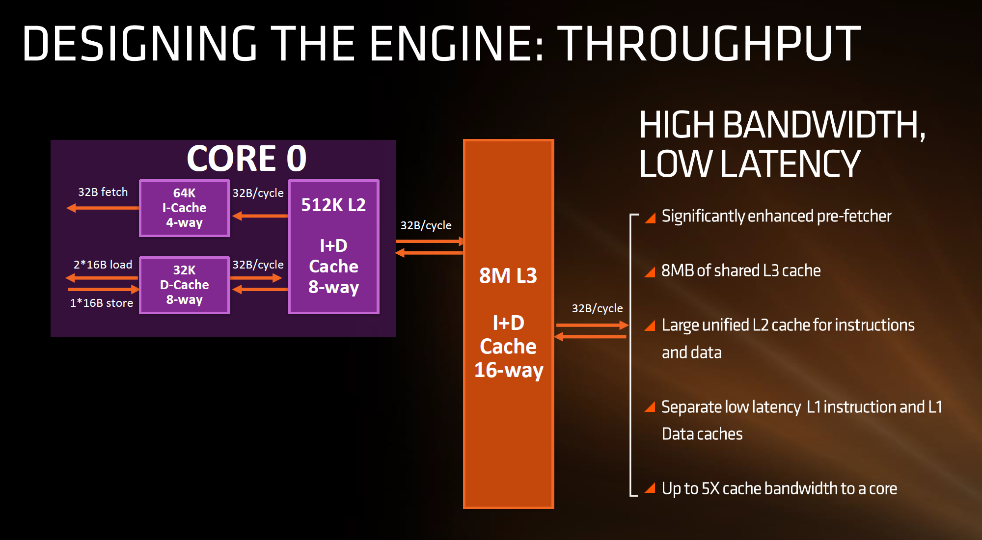
The cache hierarchy is a significant deviation from recent previous AMD designs, and most likely to its advantage. The L1 data cache is both double in size and increased in associativity compared to Bulldozer, as well as being write-back rather than write-through. It also uses an asymmetric load/store implementation, identifying that loads happen more often than stores in the critical paths of most work flows. The instruction cache is no longer shared between two cores as well as doubling in associativity, which should decrease the proportion of cache misses. AMD states that both the L1-D and L1-I are low latency, with details to come.
The L2 cache sits at half a megabyte per core with 8-way associativity, which is double that of Intel’s Skylake which has 256 KB/core and is only 4-way. On the other hand, Intel’s L3/LLC on their high-end Skylake SKUs is at 2 MB/core or 8 MB/CPU, whereas Zen will feature 1 MB/core and both are at 16-way associativity.
Edit 7:18am: Actually, the slide above is being slightly evasive in its description. It doesn't say how many cores the L3 cache is stretched over, or if there is a common LLC between all cores in the chip. However, we have recieved information from a source (which can't be confirmed via public AMD documents) that states that Zen will feature two sets of 8MB L3 cache between two groups of four cores each, giving 16 MB of L3 total. This would means 2 MB/core, but it also implies that there is no last-level unified cache in silicon across all cores, which Intel has. The reasons behind something like this is typically to do with modularity, and being able to scale a core design from low core counts to high core counts. But it would still leave a Zen core with the same L3 cache per core as Intel.
| Cache Levels | ||||
| Bulldozer FX-8150 |
Zen | Broadwell-E i7-6950X |
Skylake i7-6700K |
|
| L1 Instruction | 64 KB 2-way per module |
64 KB 4-way | 32 KB 8-way | 32 KB 8-way |
| L1 Data | 16 KB 4-way Write Through |
32 KB 8-way Write Back |
32 KB 8-way Write-Back |
32 KB 8-way Write-Back |
| L2 | 2 MB 16-way per module |
512 KB 8-way | 256 KB 8-way | 256 KB 4-way |
| L3 | 1 MB/core 64-way |
1 or 2 MB/core ? 16-way |
2.5 MB/core 16/20-way |
2 MB/core 16-way |
What this means, between the L2 and the L3, is that AMD is putting more lower level cache nearer the core than Intel, and as it is low level it becomes separate to each core which can potentially improve single thread performance. The downside of bigger and lower (but separate) caches is how each of the cores will perform snoop in each other’s large caches to ensure clean data is being passed around and that old data in L3 is not out-of-date. AMD’s big headline number overall is that Zen will offer up to 5x cache bandwidth to a core over previous designs.


216 Comments
View All Comments
MonkeyPaw - Thursday, August 18, 2016 - link
Heck, people are forgetting some significant firsts for AMD--the first to bring the IMC and hypertransport to x86. Both were big for the server world, too.smilingcrow - Friday, August 19, 2016 - link
Innovation is good and AMD have had many moments in the sun but let's not forget that Core 2 duo lacked an IMC and still trounced the AMD competition.Good products matter more than innovation and the trick is to turn innovation into good products.
The_Countess - Saturday, August 20, 2016 - link
and lets not forget the first with a on-die memory controller for a x86 CPU. a huge improvement on both the desktop and the server space. it basically is what made more then 2 socket motherboards viable at all.Kevin G - Saturday, August 20, 2016 - link
Intel had a 386 chip with an integrated memory controller back in 90's so AMD wasn't the first to do it even in the x86 segment.looncraz - Saturday, August 20, 2016 - link
Pretty sure they did not, they had memory management techs built-in, but not memory controllers. The 286 had memory management capabilities as well, and so did all of AMD's comparable CPUs, naturally.The_Countess - Sunday, August 21, 2016 - link
that would be the first time i heard about that so: source?Kevin G - Sunday, August 21, 2016 - link
80386EX for the embedded market. Came out in 1994. By this time, it was two generations behind the Pentium so it generated very little fan fair.http://news.softpedia.com/news/Intel-Wants-The-Emb...
Here is a book that includes some details about the 80386EX, though you'll have to do a bit of digging in it:
http://userpages.umbc.edu/~squire/intel_book.pdf
Gigaplex - Thursday, August 18, 2016 - link
"AMD was first with CPU + GPU = APU."Llano came out June 2011. Intel had Westmere (January 2010) and Sandy Bridge (January 2011) before Llano. Even if you discount Westmere since they were separate dies on the same package, Sandy Bridge still got there before Llano.
Mahigan - Thursday, August 18, 2016 - link
https://www.sec.gov/Archives/edgar/data/2488/00011...Intel and AMD have a cross-licensing agreement which covers patents and technologies from both firms allowing both firms to use a rather generous amount of patents from their competitor.
Nobody copied nobody. The two companies are quite intertwined tbh.
Mahigan - Thursday, August 18, 2016 - link
"Advanced Micro Devices has clarified terms of the cross-license agreement with Intel Corp. on Thursday. As it appears, if either AMD or Intel change their control (i.e., gets acquired), the cross-license agreement between the two companies is automatically terminated for both parties.AMD and Intel have a cross-licensing agreement, which guarantees that the companies will not pursue litigation for any potential patent infringements. The agreement covers entire patent portfolio for both companies, which includes general-purpose processors, graphics adapters and other intellectual property. For example, AMD can design and sell microprocessors compatible with Intel’s x86 instruction set architecture and featuring a variety of extensions, whereas Intel can develop and ship central processing units that utilize IP and extensions initially created by AMD . The cross-licensing agreement has a number of terms and limitations. For example, the chip designers are not allowed to build processors that are compatible with competitor’s infrastructure (e.g., sockets, mainboards, etc.). Besides, if AMD and Intel change their ownership , the agreement terminated."
http://www.kitguru.net/components/cpu/anton-shilov...