AMD Zen Microarchitecture: Dual Schedulers, Micro-Op Cache and Memory Hierarchy Revealed
by Ian Cutress on August 18, 2016 9:00 AM EST
In their own side event this week, AMD invited select members of the press and analysts to come and discuss the next layer of Zen details. In this piece, we’re discussing the microarchitecture announcements that were made, as well as a look to see how this compares to previous generations of AMD core designs.
AMD Zen
Prediction, Decode, Queues and Execution
First up, let’s dive right into the block diagram as shown:
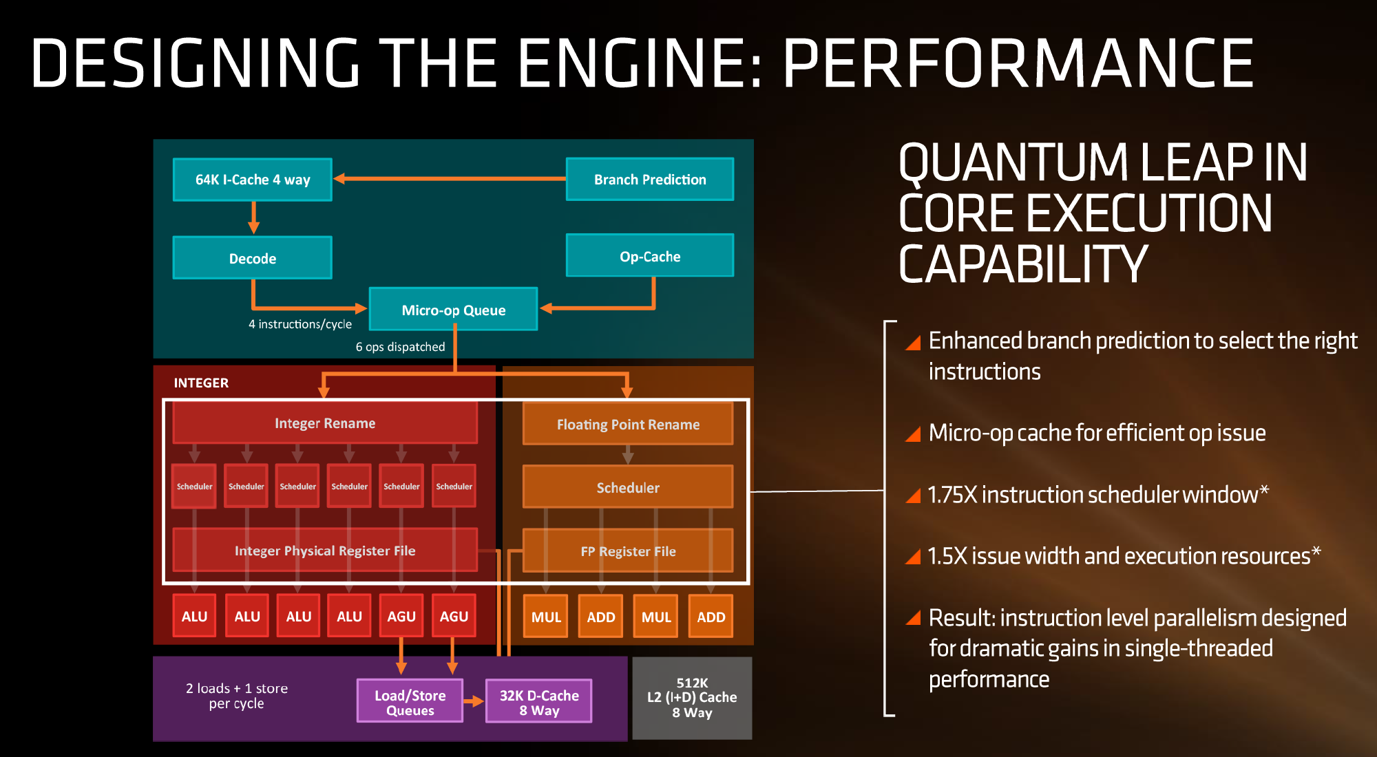
If we focus purely on the left to start, we can see most of the high-level microarchitecture details including basic caches, the new inclusion of an op-cache, some details about decoders and dispatch, scheduler arrangements, execution ports and load/store arrangements. A number of slides later in the presentation talk about cache bandwidth.
Firstly, one of the bigger deviations from previous AMD microarchitecture designs is the presence of a micro-op cache (it might be worth noting that these slides sometimes say op when it means micro-op, creating a little confusion). AMD’s Bulldozer design did not have an operation cache, requiring it to fetch details from other caches to implement frequently used micro-ops. Intel has been implementing a similar arrangement for several generations to great effect (some put it as a major stepping stone for Conroe), so to see one here is quite promising for AMD. We weren’t told the scale or extent of this buffer, and AMD will perhaps give that information in due course.
Aside from the as-expected ‘branch predictor enhancements’, which are as vague as they sound, AMD has not disclosed the decoder arrangements in Zen at this time, but has listed that they can decode four instructions per cycle to feed into the operations queue. This queue, with the help of the op-cache, can deliver 6 ops/cycle to the schedulers. The reasons behind the queue being able to dispatch more per cycle is if the decoder can supply an instruction which then falls into two micro-ops (which makes the instruction vs micro-op definitions even muddier). Nevertheless, this micro-op queue helps feed the separate integer and floating point segments of the CPU. Unlike Intel who uses a combined scheduler for INT/FP, AMD’s diagram suggests that they will remain separate with their own schedulers at this time.
The INT side of the core will funnel the ALU operations as well as the AGU/load and store ops. The load/store units can perform 2 16-Byte loads and one 16-Byte store per cycle, making use of the 32 KB 8-way set associative write-back L1 Data cache. AMD has explicitly made this a write back cache rather than the write through cache we saw in Bulldozer that was a source of a lot of idle time in particular code paths. AMD is also stating that the load/stores will have lower latency within the caches, but has not explained to what extent they have improved.
The FP side of the core will afford two multiply ports and two ADD ports, which should allow for two joined FMAC operations or one 256-bit AVX per cycle. The combination of the INT and FP segments means that AMD is going for a wide core and looking to exploit a significant amount of instruction level parallelism. How much it will be able to depends on the caches and the reorder buffers – no real data on the buffers has been given at this time, except that the cores will have a +75% bigger instruction scheduler window for ordering operations and a +50% wider issue width for potential throughput. The wider cores, all other things being sufficient, will also allow AMD’s implementation of simultaneous multithreading to potentially take advantage of multiple threads with a linear and naturally low IPC.


216 Comments
View All Comments
FMinus - Thursday, August 18, 2016 - link
He's right tho. AMD was a licensee of Intel to produce bulk Intel products, because intel couldn't keep up with the demand. Then AMD reverse engineered Intels products and brought their own line out and Intel didn't like that, thus they broke the agreement, which in the end didn't help much since AMD had already all they needed.That being said, what AMD did anyone would, so it's just business as per usual. Then they actually stepped up and made great own CPUs to combat intel and made a great dual core and AMD64. AMD did a lot for computing, but the early days were pretty much a contractor and pirate.
I wish them all the best with Zen and future, and I hope they get Vega right, by that I mean don't fucking gimp the chip by power delivery, cause you can't get that under control, everyone knows nvidia is ahead in that game, just give a great performing GPU on the market and let it eat 250W if need be.
Nagorak - Thursday, August 18, 2016 - link
Yeah, they matched Intel on the CPU front, and Intel responded by abusing their stronger market position to limit AMD's gains. I'll be happy to get an AMD processor back in my machine just based on principle.Klimax - Saturday, August 20, 2016 - link
Correction: IBM forced Intel to license number of CPU manufactures. (At least two suppliers, similar to rule sued by militaries) And there was lawsuit or two. Fun stuff.looncraz - Thursday, August 18, 2016 - link
Maybe you are too young to remember, but AMD has historically been a primary driver in processor innovation.They created the first native multi-core dies, broke the Ghz barrier, first to debut dynamic clock speeds, invented the seamless x64 transition and AMD64 instruction set, created CMT, created HSA, created the APU, and so much more. And I'm only focusing on CPUs, here.
Intel uses a great deal of AMD tech, and vice-versa.
smilingcrow - Thursday, August 18, 2016 - link
I used to buy AMD exclusively but they have been second rate for 10 years now.I don't buy innovations I buy products and AMD have really struggled for a decade to offer decent products unless your main criteria is value.
Value is fine but for mobile products where power consumption is very important and for workstations where performance is king AMD have had nothing to compete.
I'm very glad that Zen is looking as if it will compete at the higher end although I think they will find it harder to compete with Core M.
Just because I don't view AMD through ten year old rose tinted glasses doesn't mean I don't want them to succeed.
I have been feeling confident for Zen as an 8c/16t chips for ages but it's how it does as a 4c/8t chip that may well be more important in the consumer space unless the 8c/16c chip is unusually cheap for its performance level which it could even be.
Some people here can't tell the difference between someone who is critical of AMD's failings and an Intel fanboy. Intel have their issues but they have delivered decent chips in the decade that AMD fell into disarray. I'm not loyal to incompetent companies.
Nagorak - Thursday, August 18, 2016 - link
It's been hard for anyone to stick with AMD for the last decade. Phenom and Phenom II came up short, and then Bulldozer turned out to be a total disaster. In retrospect AMD should have tossed Bulldozer in the trash and started work on a new processor design immediately. Trying to iterate on that failed design is what almost killed AMD.Gigaplex - Thursday, August 18, 2016 - link
"Created the APU".That's not entirely accurate. Intel was actually first to market with their "APU" type CPUs, even though AMD announced theirs first.
KPOM - Friday, August 19, 2016 - link
These days ARM (soon SoftBank) is the company that keeps Intel management up at night. Intel missed the boat on mobile.Kevin G - Saturday, August 20, 2016 - link
The first dual core chip was POWER4 from IBM.Dynamic clock speeds existed in mobile (think ARM/MIPS) designs back in the 90's.
Seamless x86 transition could be credited to Transmeta for thei VLIW based Crusoe line of chips running x86 code. Runner up could be the FX32! emulator that ran unmodifed x86 Windows binaries in Alpha based hardware back in the 90's.
CMT was done beforehand in Sun's Niagra chip. There designs even before that did unit sharing for CMT.
Elements of HSA came from 3Dlabs and their cards supporting a unified virtual address space.
Integrating a CPU and GPU was first done by Intel though they never shipped it due to relaying on a flawed RDRAM to SDRAM buffer chip:
http://m.theregister.co.uk/2007/02/06/forgotten_te...
Thus the only innovation on your list is the 1 Ghz clock rate for a CPU, which isn't that innovative.
Klimax - Saturday, August 20, 2016 - link
Sorry, wrong. Multicores weren't AMD''s invention, dynamic clock speeds were parallel execution, x64 transition si AMD win only thanks to Microsoft who killed Intel's own development, CMT is not AMD¨s invention (and I would say it is nothing to be proud of), HSA is just label for preexisting technologies, APU was done before AMD's own (in fact, Intel had APU-like chip in late 80s),. AMD didn't invent much as most of technologies were bought in previous acquisitions like HyperTransport (See DEC Alpha)Sorry, to tell you, but what you posit is pure fantasy. AMD inveted very few things and fewer of them were of much importance or use.