AMD Zen Microarchitecture: Dual Schedulers, Micro-Op Cache and Memory Hierarchy Revealed
by Ian Cutress on August 18, 2016 9:00 AM ESTDeciphering the New Cache Hierarchy
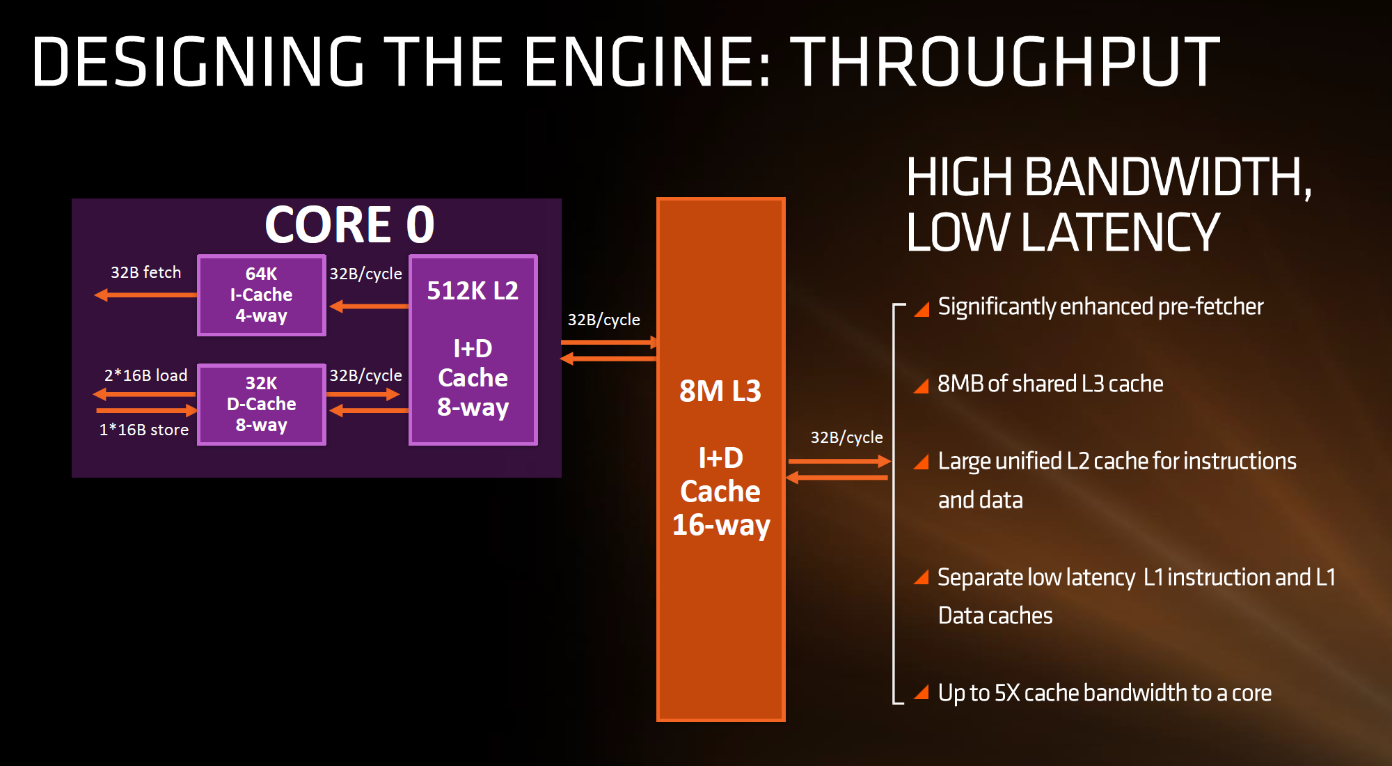
The cache hierarchy is a significant deviation from recent previous AMD designs, and most likely to its advantage. The L1 data cache is both double in size and increased in associativity compared to Bulldozer, as well as being write-back rather than write-through. It also uses an asymmetric load/store implementation, identifying that loads happen more often than stores in the critical paths of most work flows. The instruction cache is no longer shared between two cores as well as doubling in associativity, which should decrease the proportion of cache misses. AMD states that both the L1-D and L1-I are low latency, with details to come.
The L2 cache sits at half a megabyte per core with 8-way associativity, which is double that of Intel’s Skylake which has 256 KB/core and is only 4-way. On the other hand, Intel’s L3/LLC on their high-end Skylake SKUs is at 2 MB/core or 8 MB/CPU, whereas Zen will feature 1 MB/core and both are at 16-way associativity.
Edit 7:18am: Actually, the slide above is being slightly evasive in its description. It doesn't say how many cores the L3 cache is stretched over, or if there is a common LLC between all cores in the chip. However, we have recieved information from a source (which can't be confirmed via public AMD documents) that states that Zen will feature two sets of 8MB L3 cache between two groups of four cores each, giving 16 MB of L3 total. This would means 2 MB/core, but it also implies that there is no last-level unified cache in silicon across all cores, which Intel has. The reasons behind something like this is typically to do with modularity, and being able to scale a core design from low core counts to high core counts. But it would still leave a Zen core with the same L3 cache per core as Intel.
| Cache Levels | ||||
| Bulldozer FX-8150 |
Zen | Broadwell-E i7-6950X |
Skylake i7-6700K |
|
| L1 Instruction | 64 KB 2-way per module |
64 KB 4-way | 32 KB 8-way | 32 KB 8-way |
| L1 Data | 16 KB 4-way Write Through |
32 KB 8-way Write Back |
32 KB 8-way Write-Back |
32 KB 8-way Write-Back |
| L2 | 2 MB 16-way per module |
512 KB 8-way | 256 KB 8-way | 256 KB 4-way |
| L3 | 1 MB/core 64-way |
1 or 2 MB/core ? 16-way |
2.5 MB/core 16/20-way |
2 MB/core 16-way |
What this means, between the L2 and the L3, is that AMD is putting more lower level cache nearer the core than Intel, and as it is low level it becomes separate to each core which can potentially improve single thread performance. The downside of bigger and lower (but separate) caches is how each of the cores will perform snoop in each other’s large caches to ensure clean data is being passed around and that old data in L3 is not out-of-date. AMD’s big headline number overall is that Zen will offer up to 5x cache bandwidth to a core over previous designs.


216 Comments
View All Comments
JoeyJoJo123 - Thursday, August 18, 2016 - link
The ignorance... It hurts...Original x86 (32-bit) was Intel-AMD developed.
AMD then developed x86-64, or x86 64-bit, and then Intel continues to license it to this day.
There's no copying here. Someone did it first, then others are licensing that IP from them.
See: https://en.wikipedia.org/wiki/X86-64
>x86-64 (also known as x64, x86_64 and AMD64) is the 64-bit version of the x86 instruction set.
>The original specification, created by AMD and released in 2000, has been implemented by AMD, Intel and VIA.
That's why sometimes you might see driver versions labeled AMD64, and you might be puzzled as to why despite being on a Intel 64-bit CPU that the 64-bit driver you downloaded states AMD64 in the name. It's because it was an AMD-first technology, but it's usable on any x86-64bit processor.
Bateluer - Thursday, August 18, 2016 - link
Intel simply paid for the license to copy the technology AMD designed. They still copied it, just legally paid for the right to do so.Klimax - Saturday, August 20, 2016 - link
Actually, not exactly correct. Intel was forced by Microsoft to adopt AMD's solution, despite Intel having parallel own implementation which was different. And Intel's version is still bit different from AMD's. (Some instructions are different between implementations, mostly relevant only to OS)xenol - Thursday, August 18, 2016 - link
IBM made the dual-core on a single die design.ExarKun333 - Thursday, August 18, 2016 - link
In many ways, Intel's 64-bit was superior to AMD's, but x86-64 was more backward compatible. I can see it both ways....different solutions to the same problem. Both companies have pushed each other...TheMightyRat - Thursday, August 18, 2016 - link
How is IA64 superior to AMD64?AMD64 can run 32-bit software without performance hit and still run 64-bit software comparatively equally to Intel counterpart.
IA64 Itanium runs 64-bit software much slower than a Pentium 4 64-bit at the same clock and has a massive performance hit in 32-bit emulation (1/3 as fast). Aren't both of them based on Netburst?
EMT64 only has more codes than AMD64 as it also implement both AMD64 and IA64, which is no longer used in modern server software anymore.
Klimax - Saturday, August 20, 2016 - link
He was talking about Intel's x64 which was backup plan in case Itanium fails.Myrandex - Thursday, August 25, 2016 - link
I don't think Itaniums were Netburst in architecture, it seemed to be a totally different architecture.Gigaplex - Thursday, August 18, 2016 - link
Itanium was novel but turned out to be a poor performer. It relied too much on good compilers optimising the instruction order.KPOM - Friday, August 19, 2016 - link
Wasn't Itanium based on "Very Long Instruction Word" architecture? Hence the long pipelines and reliance on clock speed? The Pentium M from Intel Israel righted Intel's ship and allowed them to take leadership of the x86 architecture back from AMD.