Hidden Secrets: Investigation Shows That NVIDIA GPUs Implement Tile Based Rasterization for Greater Efficiency
by Ryan Smith on August 1, 2016 5:00 AM EST
As someone who analyzes GPUs for a living, one of the more vexing things in my life has been NVIDIA’s Maxwell architecture. The company’s 28nm refresh offered a huge performance-per-watt increase for only a modest die size increase, essentially allowing NVIDIA to offer a full generation’s performance improvement without a corresponding manufacturing improvement. We’ve had architectural updates on the same node before, but never anything quite like Maxwell.
The vexing aspect to me has been that while NVIDIA shared some details about how they improved Maxwell’s efficiency over Kepler, they have never disclosed all of the major improvements under the hood. We know, for example, that Maxwell implemented a significantly altered SM structure that was easier to reach peak utilization on, and thanks to its partitioning wasted much less power on interconnects. We also know that NVIDIA significantly increased the L2 cache size and did a number of low-level (transistor level) optimizations to the design. But NVIDIA has also held back information – the technical advantages that are their secret sauce – so I’ve never had a complete picture of how Maxwell compares to Kepler.
For a while now, a number of people have suspected that one of the ingredients of that secret sauce was that NVIDIA had applied some mobile power efficiency technologies to Maxwell. It was, after all, their original mobile-first GPU architecture, and now we have some data to back that up. Friend of AnandTech and all around tech guru David Kanter of Real World Tech has gone digging through Maxwell/Pascal, and in an article & video published this morning, he outlines how he has uncovered very convincing evidence that NVIDIA implemented a tile based rendering system with Maxwell.
In short, by playing around with some DirectX code specifically designed to look at triangle rasterization, he has come up with some solid evidence that NVIDIA’s handling of tringles has significantly changed since Kepler, and that their current method of triangle handling is consistent with a tile based renderer.
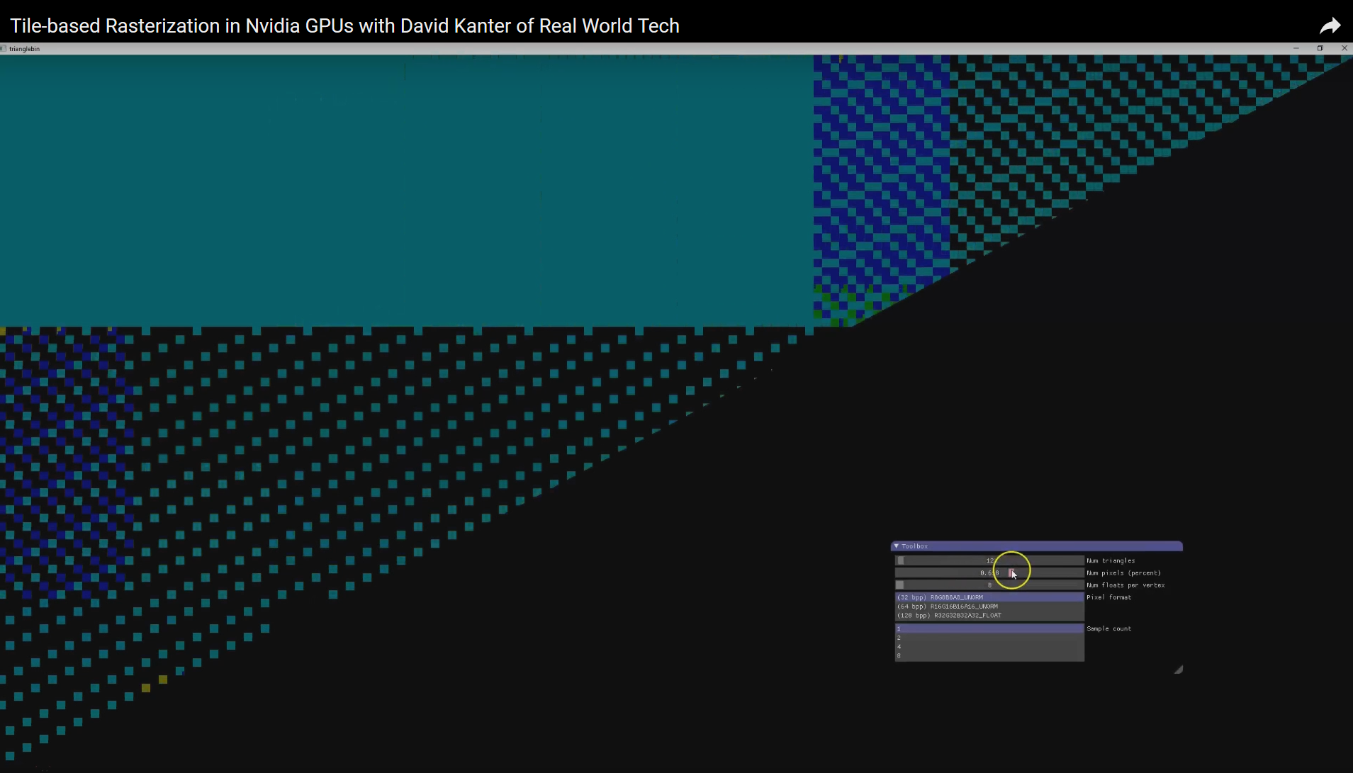
NVIDIA Maxwell Architecture Rasterization Tiling Pattern (Image Courtesy: Real World Tech)
Tile based rendering is something we’ve seen for some time in the mobile space, with both Imagination PowerVR and ARM Mali implementing it. The significance of tiling is that by splitting a scene up into tiles, tiles can be rasterized piece by piece by the GPU almost entirely on die, as opposed to the more memory (and power) intensive process of rasterizing the entire frame at once via immediate mode rendering. The trade-off with tiling, and why it’s a bit surprising to see it here, is that the PC legacy is immediate mode rendering, and this is still how most applications expect PC GPUs to work. So to implement tile based rasterization on Maxwell means that NVIDIA has found a practical means to overcome the drawbacks of the method and the potential compatibility issues.
In any case, Real Word Tech’s article goes into greater detail about what’s going on, so I won’t spoil it further. But with this information in hand, we now have a more complete picture of how Maxwell (and Pascal) work, and consequently how NVIDIA was able to improve over Kepler by so much. Finally, at this point in time Real World Tech believes that NVIDIA is the only PC GPU manufacturer to use tile based rasterization, which also helps to explain some of NVIDIA’s current advantages over Intel’s and AMD’s GPU architectures, and gives us an idea of what we may see them do in the future.
Source: Real World Tech


191 Comments
View All Comments
Yojimbo - Tuesday, August 2, 2016 - link
Ehh, I could be wrong but from what I remember AMD had driver issues at the time. NVIDIA has just consistently had a more complete and polished product lineup. Certain cards or generations may have turned out better than others for AMD, but you're gonna be less likely to buy a product when the previous generation had problems X and Y. A company must execute consistently to maintain enough momentum to win market share in gaming graphics because the brands are very well known by the buyers.. In that sense it is a sort of branding issue. But it's not a marketing issue, unlike what a lot of people tend to imply when they disdainfully dismiss it as a branding issue.wumpus - Wednesday, August 3, 2016 - link
I'm pretty sure Intel's slice (volume, not revenue) is bigger than even nVidia's. AMD is getting squeezed on both sides, a steadily decreasing chunk of a steadily decreasing market.Mr.AMD - Monday, August 1, 2016 - link
That is a nice assumption, but very wrong.AMD will show true performance in the higher levels by releasing Vega 10 and 11 GPU's.
Performance/Watt/Dollar is going to be almost perfect for AMD, rumor goes AMD will PAPER launch Vega in October. I truly can't wait for Vega, because the performance will be very high on this 16Nm FF node. Better OC, better stock performance, better every thing.
TessellatedGuy - Monday, August 1, 2016 - link
future technology is obviously gonna be better. And who knows, polaris efficiency was a big fail in efficiency. Could happen to vega as well. You made a nice assumption as well, but very wrong too.looncraz - Monday, August 1, 2016 - link
Polaris efficiency is hampered by 8 inefficient GDDR5 controllers. The 110W GPU TDP would be closer to 90W without GDDR5.The RX480 VRM uses about 20W, and the RAM uses about 30W.
With HBM2 the GPU TDP would be 95W, RAM would use 10W, and the VRM could use 15W.
That would be 120W total, vs 160W.
Scali - Monday, August 1, 2016 - link
"Polaris efficiency is hampered by 8 inefficient GDDR5 controllers."GTX1070 has the exact same memory, same 150W TDP, yet delivers a lot more performance.
AMD is clearly doing something wrong in terms of efficiency. They can move to HBM2, but so can nVidia.
JeffFlanagan - Monday, August 1, 2016 - link
Your post seemed really odd, like propaganda really. Then I noticed your user name.Chaser - Tuesday, August 2, 2016 - link
What color are those glasses?StrangerGuy - Tuesday, August 2, 2016 - link
Yeah I'm sure every AMD fanboy were saying the same thing for Bulldozer back in 2011 too.Yojimbo - Tuesday, August 2, 2016 - link
My guess is Vega will just be the Polaris architecture with more shaders. It needs the memory bandwidth of HBM whereas Pascal does not, because Pascal is a more memory bandwidth efficient architecture than Polaris. It'll have better efficiency than Polaris because of the HBM 2, but not nearly as good as Pascal because although the memory subsystem on Vega will be using less power than that of Pascal, the rest of the GPU will be using a lot more. They'll probably water cool it again so they can get the thermals necessary to run the card fast enough while staying under a reasonable TDP. In that case it will have similar issues to the Fury line. AMD needs Navi in a bad way.