Ten Year Anniversary of Core 2 Duo and Conroe: Moore’s Law is Dead, Long Live Moore’s Law
by Ian Cutress on July 27, 2016 10:30 AM EST- Posted in
- CPUs
- Intel
- Core 2 Duo
- Conroe
- ITRS
- Nostalgia
- Time To Upgrade
Core: Out of Order and Execution
After Prefetch, Cache and Decode comes Order and Execution. Without rehashing discussions of in-order vs. out-of-order architectures, typically a design with more execution ports and a larger out-of-order reorder buffer/cache can sustain a higher level of instructions per clock as long as the out-of-order buffer is smart, data can continuously be fed, and all the execution ports can be used each cycle. Whether having a super-sized core is actually beneficial to day-to-day operations in 2016 is an interesting point to discuss, during 2006 and the Core era it certainly provided significant benefits.
As Johan did back in the original piece, let’s start with semi-equivalent microarchitecture diagrams for Core vs. K8:
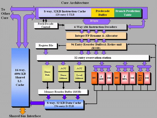
Intel Core
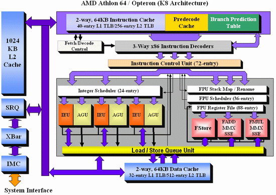
AMD K8
For anyone versed in x86 design, three differences immediately stand out when comparing the two. First is the reorder buffer, which for Intel ranks at 96 entries, compared to 72 for AMD. Second is the scheduler arrangement, where AMD uses split 24-entry INT and 36-entry FP schedulers from the ‘Instruction Control Unit’ whereas Intel has a 32-entry combined ‘reservation station’. Third is the number of SSE ports: Intel has three compared to two from AMD. Let’s go through these in order.
For the reorder buffers, with the right arrangement, bigger is usually better. Make it too big and it uses too much silicon and power however, so there is a fine line to balance between them. Also, the bigger the buffer it is, the less of an impact it has. The goal of the buffer is to push decoded instructions that are ready to work to the front of the queue, and make sure other instructions which are order dependent stay in their required order. By executing independent operations when they are ready, and allowing prefetch to gather data for instructions still waiting in the buffer, this allows latency and bandwidth issues to be hidden. (Large buffers are also key to simultaneous multithreading, which we’ll discuss in a bit as it is not here in Core 2 Duo.) However, when the buffer has the peak number of instructions being sent to the ports every cycle already, having a larger buffer has diminishing returns (the design has to keep adding ports instead, depending on power/silicon budget).
For the scheduler arrangements, using split or unified schedulers for FP and INT has both upsides and downsides. For split schedulers, the main benefit is entry count - in this case AMD can total 60 (24-INT + 36-FP) compared to Intel’s 32. However, a combined scheduler allows for better utilization, as ports are not shared between the split schedulers.
The SSE difference between the two architectures is exacerbated by what we’ve already discussed – macro-op fusion. The Intel Core microarchitecture has 3 SSE units compared to two, but also it allows certain SSE packed instructions to execute within one instruction, due to fusion, rather than two. Two of the Intel’s units are symmetric, with all three sporting 128-bit execution rather than 64-bit on K8. This means that K8 requires two 64-bit instructions whereas Intel can absorb a 128-bit instruction in one go. This means Core can outperform K8 on 128-bit SSE on many different levels, and for 64-bit FP SSE, Core can do 4 DP per cycle, whereas Athlon 64 can do 3.
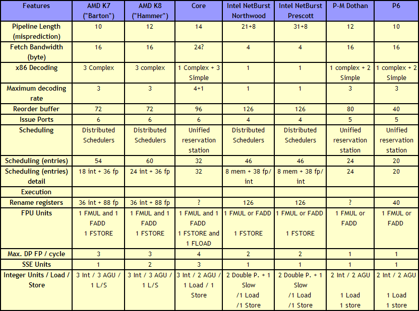
One other metric not on the diagram comes from branch prediction. Core can sustain one branch prediction per cycle, compared to one per two cycles on previous Intel microarchitectures. This was Intel matching AMD in this case, who already supported one per cycle.


158 Comments
View All Comments
Akrovah - Wednesday, July 27, 2016 - link
My old E6700 is still alive and kicking. I only just replaced it as my primary system when Devil's Canyon came along. Still use it for my four year old's "first computer."djayjp - Wednesday, July 27, 2016 - link
Not a particle physicist, nor electrical engineer, so just some pie in the sky wondering here, but wouldn't it be possible to build transistors using carbon nanotubes, or light itself (using nano sized mirrors/interferometers, like DLP) or even basing the transistor gates off of protons/sub atomic particles?michael2k - Wednesday, July 27, 2016 - link
I think a more interesting question is using glass as a substrate. Imagine printing nand, CPU, GPU, ram, and along the bezels of a smartphone.That reduces a phone to six components: a display, a transducer for sound, a mic, a battery, a radio, and a chassis, which would have all the antennas.
joex4444 - Wednesday, July 27, 2016 - link
Particle physicist here. Light has the tricky property that it travels at the speed of light so I can't imagine it working but perhaps I'm envisioning your concept differently than you are. For carbon nanotubes, you'll need a materials engineer or a condensed matter physicist.3DoubleD - Wednesday, July 27, 2016 - link
Materials/Semiconductor Physics Engineer here. The problem is not what we CAN do, the problem is what is economically possible at scale. For example, FinFETs were demonstrated at the turn of the century, but took all of those years to become (1) necessary - planar transistor were getting too leaky, and (2) possible to fabricate economically in large scales.Researchers have created smaller, faster transistors years ago, but it takes a lot of time and effort to develop the EUV or quadruple patterning technologies that enable these devices to be reliably and affordably manufactured.
So I think the problem in moving "beyond silicon" is not that we don't have alternatives, it is that we have many alternatives, we just don't know which will scale. It becomes less of a purely engineering problem and manufacturing business problem. When new technologies relied purely on the established silicon industry alone, you could reasonably extrapolate how much each new technology would cost as the nodes were scaled down. When we talk about using III-V FinFETs/ All Around Gates or graphene and carbon nanotubes, we don't really know how those things will scale with the existing processes as we move them from the laboratory to the manufacturing line.
I've been looking forward to this transition for years. People moan that it is the end of Moores Law, but that could be a good thing. Silicon is a great material for forming logic circuits for many reasons, but it also has many downsides. While silicon never reached 10 GHz (as Intel once predicted), other materials easily blow past 100 GHz transistor switching speeds. When the massive engines that work tirelessly to reduce our lithography nodes nm by nm are aimed at "the next big thing", we might be pleasantly surprised by a whole new paradigm of performance.
So what competes with modern day Si CMOS on speed, power usage, and cost? Nothing... yet!
djayjp - Thursday, July 28, 2016 - link
Yes, it's fascinating stuff. Thanks for reminding me about that. I recall now that I think it was graphene that enabled those insanely high switching speeds, due to its incredible conductivity/efficiency. Hopefully it can now be made economically feasible at some point! Imagine a the next GPU that is 10x smaller and operates at 100x the clock speed. A GTX 1080Ti x 1000! Finally we can do real time true global illumination ha....jeffry - Monday, August 1, 2016 - link
Thats a good point. Like, answering a question "are you willing to pay $800 for a new CPU to double the computers speed?" Most consumers say no. It all comes down to the mass market price.wumpus - Thursday, August 4, 2016 - link
From the birth of the Univac until 10 years ago, consumers consistently said YES! and plunked down their money. Doubling the (per thread) speed of a core2duo is going to cost more than $800. Also the cost of the RAM on servers is *WAY* more than $800, so you can expect if Intel could double the power of each core, they could crank prices up by at least $800 per core on Xeons. They can't, and neither can IBM or AMD.Jaybus - Thursday, July 28, 2016 - link
Sure, but that speed is dependent on the medium. There are some proposed optical transistors using electromagnetically induced transparency. Long way off. However, silicon photonics could change some things. Capacitance is the killer for electronic interconnects, whether chip-to-chip or on-chip bus. An optical interconnect could greatly increase bandwidth without increasing the chip's power dissipation. I think an electronic-photonic hybrid is more likely, since silicon photonics components can be made on a CMOS process. We are already beginning to see optical PCI Express being deployed. I could definitely see a 3D approach where 2D electronic layers are connected through an optical rather than electronic bus.djayjp - Thursday, July 28, 2016 - link
Yes, transparency, like polarized windows that either become transparent or opaque when a current is applied (to the liquid crystals?). I wonder how small they could be made. It would be incredibly power efficient I would think.