Ten Year Anniversary of Core 2 Duo and Conroe: Moore’s Law is Dead, Long Live Moore’s Law
by Ian Cutress on July 27, 2016 10:30 AM EST- Posted in
- CPUs
- Intel
- Core 2 Duo
- Conroe
- ITRS
- Nostalgia
- Time To Upgrade
Core: Out of Order and Execution
After Prefetch, Cache and Decode comes Order and Execution. Without rehashing discussions of in-order vs. out-of-order architectures, typically a design with more execution ports and a larger out-of-order reorder buffer/cache can sustain a higher level of instructions per clock as long as the out-of-order buffer is smart, data can continuously be fed, and all the execution ports can be used each cycle. Whether having a super-sized core is actually beneficial to day-to-day operations in 2016 is an interesting point to discuss, during 2006 and the Core era it certainly provided significant benefits.
As Johan did back in the original piece, let’s start with semi-equivalent microarchitecture diagrams for Core vs. K8:
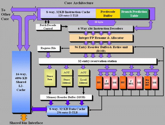
Intel Core
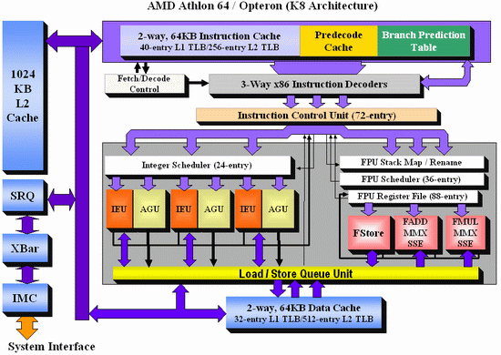
AMD K8
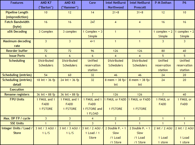
For anyone versed in x86 design, three differences immediately stand out when comparing the two. First is the reorder buffer, which for Intel ranks at 96 entries, compared to 72 for AMD. Second is the scheduler arrangement, where AMD uses split 24-entry INT and 36-entry FP schedulers from the ‘Instruction Control Unit’ whereas Intel has a 32-entry combined ‘reservation station’. Third is the number of SSE ports: Intel has three compared to two from AMD. Let’s go through these in order.
For the reorder buffers, with the right arrangement, bigger is usually better. Make it too big and it uses too much silicon and power however, so there is a fine line to balance between them. Also, the bigger the buffer it is, the less of an impact it has. The goal of the buffer is to push decoded instructions that are ready to work to the front of the queue, and make sure other instructions which are order dependent stay in their required order. By executing independent operations when they are ready, and allowing prefetch to gather data for instructions still waiting in the buffer, this allows latency and bandwidth issues to be hidden. (Large buffers are also key to simultaneous multithreading, which we’ll discuss in a bit as it is not here in Core 2 Duo.) However, when the buffer has the peak number of instructions being sent to the ports every cycle already, having a larger buffer has diminishing returns (the design has to keep adding ports instead, depending on power/silicon budget).
For the scheduler arrangements, using split or unified schedulers for FP and INT has both upsides and downsides. For split schedulers, the main benefit is entry count - in this case AMD can total 60 (24-INT + 36-FP) compared to Intel’s 32. However, a combined scheduler allows for better utilization, as ports are not shared between the split schedulers.
The SSE difference between the two architectures is exacerbated by what we’ve already discussed – macro-op fusion. The Intel Core microarchitecture has 3 SSE units compared to two, but also it allows certain SSE packed instructions to execute within one instruction, due to fusion, rather than two. Two of the Intel’s units are symmetric, with all three sporting 128-bit execution rather than 64-bit on K8. This means that K8 requires two 64-bit instructions whereas Intel can absorb a 128-bit instruction in one go. This means Core can outperform K8 on 128-bit SSE on many different levels, and for 64-bit FP SSE, Core can do 4 DP per cycle, whereas Athlon 64 can do 3.
One other metric not on the diagram comes from branch prediction. Core can sustain one branch prediction per cycle, compared to one per two cycles on previous Intel microarchitectures. This was Intel matching AMD in this case, who already supported one per cycle.


158 Comments
View All Comments
saratoga4 - Wednesday, July 27, 2016 - link
>As we can see, by 2007 it was predicted that we would be on 10nm chipsShould be 100 nm (0.1 microns).
Jehab - Wednesday, July 27, 2016 - link
Yeah, that is a massive error, lol.hammer256 - Wednesday, July 27, 2016 - link
If I remember correctly, intel was running at 65nm in 2007 right? So I guess that was ahead of the curve at the time.JlHADJOE - Saturday, July 30, 2016 - link
And the 2001 ITR roadmap actually predicted 22nm for 2016. Despite the delays getting to 14/16nm the industry is actually way ahead of the curve.http://www2.lbl.gov/Science-Articles/Archive/ALS-E...
melgross - Wednesday, July 27, 2016 - link
Exactly! I was going to post that myself. Once it's understood that it's actually 100nm, the other numbers make sense, otherwise, they don't.Walkermoon - Wednesday, July 27, 2016 - link
Just signed up to say the same.Ian Cutress - Wednesday, July 27, 2016 - link
Derp, I misread the table in a rush. Updated.Pissedoffyouth - Wednesday, July 27, 2016 - link
Could you bench it against an AMD A10 Kaveri? That would be goodGc - Saturday, July 30, 2016 - link
AMD A10-7800 (Kaveri) is in three of the bar charts on page 6. It appears to benefit from 4 cores in two of the comparisons.Zaxx420 - Wednesday, July 27, 2016 - link
Still have a E8400 rig that I use every day...with it o/ced to 4GHz, 8gb of DDR2-1066 and a OCZ Vertex 2 SSD plus it's 6mb of cache on a P45 mobo...it can hold its own to this day...easily. The E8000 series is one of the best 'future proof' cpus ever...next up imo will prove to be Sandy Bridge. Have a 2500K at 4.5GHz on a Z68 mobo, 16gb DDR3-2400 and a Samsung 850 Pro ssd...and now a GTX 1060...plays any game I want at 1080 and max quality...easily.