Ten Year Anniversary of Core 2 Duo and Conroe: Moore’s Law is Dead, Long Live Moore’s Law
by Ian Cutress on July 27, 2016 10:30 AM EST- Posted in
- CPUs
- Intel
- Core 2 Duo
- Conroe
- ITRS
- Nostalgia
- Time To Upgrade
Core: Decoding, and Two Goes Into One
The role of the decoder is to decipher the incoming instruction (opcode, addresses), and translate the 1-15 byte variable length instruction into a fixed-length RISC-like instruction that is easier to schedule and execute: a micro-op. The Core microarchitecture has four decoders – three simple and one complex. The simple decoder can translate instructions into single micro-ops, while the complex decoder can convert one instruction into four micro-ops (and long instructions are handled by a microcode sequencer). It’s worth noting that simple decoders are lower power and have a smaller die area to consider compared to complex decoders. This style of pre-fetch and decode occurs in all modern x86 designs, and by comparison AMD’s K8 design has three complex decoders.
The Core design came with two techniques to assist this part of the core. The first is macro-op fusion. When two common x86 instructions (or macro-ops) can be decoded together, they can be combined to increase throughput, and allows one micro-op to hold two instructions. The grand scheme of this is that four decoders can decode five instructions in one cycle.
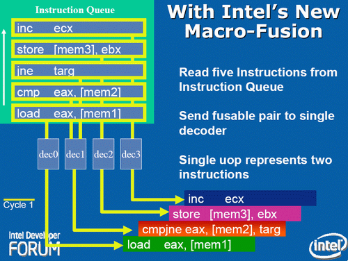
According to Intel at the time, for a typical x86 program, 20% of macro-ops can be fused in this way. Now that two instructions are held in one micro-op, further down the pipe this means there is more decode bandwidth for other instructions and less space taken in various buffers and the Out of Order (OoO) queue. Adjusting the pipeline such that 1-in-10 instructions are fused with another instruction should account for an 11% uptick in performance for Core. It’s worth noting that macro-op fusion (and macro-op caches) has become an integral part of Intel’s microarchitecture (and other x86 microarchitectures) as a result.
The second technique is a specific fusion of instructions related to memory addresses rather than registers. An instruction that requires an addition of a register to a memory address, according to RISC rules, would typically require three micro-ops:
| Pseudo-code | Instructions |
| read contents of memory to register2 | MOV EBX, [mem] |
| add register1 to register2 | ADD EBX, EAX |
| store result of register2 back to memory | MOV [mem], EBX |
However, since Banias (after Yonah) and subsequently in Core, the first two of these micro-ops can be fused. This is called micro-op fusion. The pre-decode stage recognizes that these macro-ops can be kept together by using smarter but larger circuitry without lowering the clock frequency. Again, op fusion helps in more ways than one – more throughput, less pressure on buffers, higher efficiency and better performance. Alongside this simple example of memory address addition, micro-op fusion can play heavily in SSE/SSE2 operations as well. This is primarily where Core had an advantage over AMD’s K8.
AMD’s definitions of macro-ops and micro-ops differ to that of Intel, which makes it a little confusing when comparing the two:
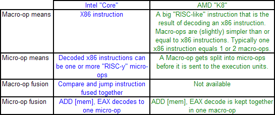
However, as mentioned above, AMD’s K8 has three complex decoders compared to Core’s 3 simple + 1 complex decoder arrangement. We also mentioned that simple decoders are smaller, use less power, and spit out one Intel micro-op per incoming variable length instruction. AMD K8 decoders on the other hand are dual purpose: it can implement Direct Path decoding, which is kind of like Intel’s simple decoder, or Vector decoding, which is kind of like Intel’s complex decoder. In almost all circumstances, the Direct Path is preferred as it produces fewer ops, and it turns out most instructions go down the Direct Path anyway, including floating point and SSE instructions in K8, resulting in fewer instructions over K7.
While extremely powerful in what they do, AMD’s limitation for K8, compared to Intel’s Core, is two-fold. AMD cannot perform Intel’s version of macro-op fusion, and so where Intel can pack one fused instruction to increase decode throughput such as the load and execute operations in SSE, AMD has to rely on two instructions. The next factor is that by virtue of having more decoders (4 vs 3), Intel can decode more per cycle, which expands with macro-op fusion – where Intel can decode five instructions per cycle, AMD is limited to just three.
As Johan pointed out in the original article, this makes it hard for AMD’s K8 to have had an advantage here. It would require three instructions to be fetched for the complex decoder on Intel, but not kick in the microcode sequencer. Since the most frequent x86 instructions map to one Intel micro-op, this situation is pretty unlikely.


158 Comments
View All Comments
Ian Cutress - Tuesday, August 2, 2016 - link
To clarify, there was a typo in Johan's original review of the microarchitecture, specifically stating:'However, Core is clearly a descendant of the Pentium Pro,'
I've updated the article to reflect this, and was under the assumption that my source was correct at the point of doing my research.
wumpus - Tuesday, August 2, 2016 - link
Except that the Pentium Pro was the first chip with the P6 architecture. Pentium 2 was pretty much pentium pro with MMX, a higher clock rate, and slower [off chip but on slot] L2 cache. Pentium 3 was the same with more clock, more MMX (possibly SSE), and on chip (full speed) L2 cache.While I'd have to assume they would pull all the files from the Pentium 3 plans, I'd still call it "pentinium pro based" because that was where nearly all the architecture came from (with minor upgrades and bug fixes to the core in 2 and 3).
I'm still curious as to exactly how they pulled it off. My main theory is that they duplicated the block diagram of the P6, and then verified each block was correct (and exactly duplicated the P6 at a higher speed), then used the P6 verification to prove that if the blocks were all correct, they had a correct chip.
zodiacfml - Thursday, July 28, 2016 - link
Same here. I thought it was the design of the Pentium M (from Israel team) they got the Core from. It was that time that AMD is beating Intel's P4's in performance, efficiency, and price. After a few months, articles were posted with people able to overclock a Pentium M with the characteristics of the AMD CPU and, of course, beating Pentium 4's at much lower clock speeds. From there, the Intel Core was born out of the Pentium M's which is essentially the same only with higher TDP and clock speeds. Then came, the Core Duo, then the Core 2 Duo.I just can't remember where I read it though.
marty1980 - Wednesday, July 27, 2016 - link
I started college in electrical engineering; moved to software after an ee class using c++. I was very excited and confident in a DIY PC. I knew the Core 2 was on its way. I gathered parts from whatever computers I could scratch together; power supply, case, DVD drive, network card(s), HDDs ... Everything but Mobo, CPU, GPU and RAM - the brains.I bought an E6400 2.13GHz with a gigabyte mobo, 4GB 800MHz DDR2 and a Radeon x1650 Pro.
I just retired the CPU and Mobo in 2012/13 when I experimented with my current PC; an AMD APU + Ded GPU (dual graphics).
I'm excited to be looking at a future replacement for my PC. We're on the horizon of some interesting changes that I don't even understand (what was his article about? Lol).
just4U - Thursday, July 28, 2016 - link
I seem to recall from a casual glance at an article (on this site) back some 9 years ago.. That intel basically got lucky, or fluked as it were.. Something to do with what they were doing with the PentiumM which caused them to move away from the P3-4 stuff.. hum.. damned if I can remember though what it was about.FourEyedGeek - Tuesday, August 9, 2016 - link
Pentium 3 architecture was having difficulties increasing performance so they replaced it with Pentium 4s Netburst. They had their Israel department continue work on Pentium 3 that turned into the Pentium M.Hazly79 - Thursday, July 28, 2016 - link
surprised that my 2005-Pentium D 3ghz still can run Diablo 3 (2012) at minimum setting pair with Nvidia GT 710 ($35 card )Really great optimization from Blizzard ent. team...
AnnonymousCoward - Thursday, July 28, 2016 - link
Yeah, but too bad the game sucks. Jay doubled it.name99 - Thursday, July 28, 2016 - link
Two points:Firstly macro-op fusion is hardly an x86 exclusive these days. Many (all?) ARMv8 CPUs use it, as do the most recent POWER CPUs. Like the x86 case, it's used to fuse together pairs of instructions that commonly co-occur. Compare and branch is a common example, but other common examples in RISC are instruction pairs that are used to create large constants in a register, or to generate large constant offsets for loads/stores.
Secondly you suggest that the ROB is an expensive data structure. This is misleading. The ROB itself is primarily a FIFO and can easily be grown. The problem is that storing more items in the ROB requires more physical registers and more load/store queue entries, and it is THESE structures that are difficult and expensive to grow. This suggests that using alternative structures for the load/store queues, and alternative mechanisms for scavenging physical registers could allow for much larger ROBs, and in fact Intel has published a lot of work on this (but has so far done apparently nothing with this research, even though the first such publications were late 90s --- I would not be surprised if Apple provides us with a CPU implementing these ideas before Intel does).
Ian Cutress - Tuesday, August 2, 2016 - link
It wasn't written about to the exclusion of all other microarchitectures, it was written about focusing on x86 back in 2006. At the time, the ROB was described as expensive by Intel, through I appreciate that might have changed.