Ten Year Anniversary of Core 2 Duo and Conroe: Moore’s Law is Dead, Long Live Moore’s Law
by Ian Cutress on July 27, 2016 10:30 AM EST- Posted in
- CPUs
- Intel
- Core 2 Duo
- Conroe
- ITRS
- Nostalgia
- Time To Upgrade
Core: Decoding, and Two Goes Into One
The role of the decoder is to decipher the incoming instruction (opcode, addresses), and translate the 1-15 byte variable length instruction into a fixed-length RISC-like instruction that is easier to schedule and execute: a micro-op. The Core microarchitecture has four decoders – three simple and one complex. The simple decoder can translate instructions into single micro-ops, while the complex decoder can convert one instruction into four micro-ops (and long instructions are handled by a microcode sequencer). It’s worth noting that simple decoders are lower power and have a smaller die area to consider compared to complex decoders. This style of pre-fetch and decode occurs in all modern x86 designs, and by comparison AMD’s K8 design has three complex decoders.
The Core design came with two techniques to assist this part of the core. The first is macro-op fusion. When two common x86 instructions (or macro-ops) can be decoded together, they can be combined to increase throughput, and allows one micro-op to hold two instructions. The grand scheme of this is that four decoders can decode five instructions in one cycle.
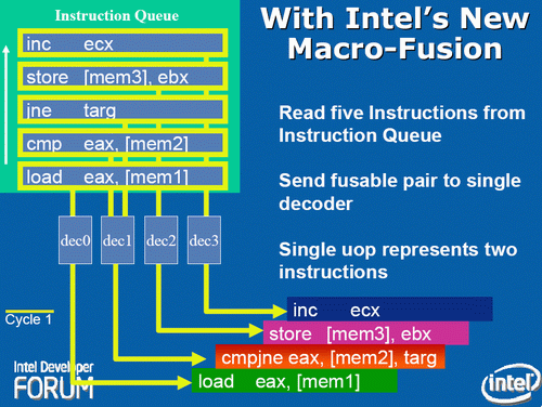
According to Intel at the time, for a typical x86 program, 20% of macro-ops can be fused in this way. Now that two instructions are held in one micro-op, further down the pipe this means there is more decode bandwidth for other instructions and less space taken in various buffers and the Out of Order (OoO) queue. Adjusting the pipeline such that 1-in-10 instructions are fused with another instruction should account for an 11% uptick in performance for Core. It’s worth noting that macro-op fusion (and macro-op caches) has become an integral part of Intel’s microarchitecture (and other x86 microarchitectures) as a result.
The second technique is a specific fusion of instructions related to memory addresses rather than registers. An instruction that requires an addition of a register to a memory address, according to RISC rules, would typically require three micro-ops:
| Pseudo-code | Instructions |
| read contents of memory to register2 | MOV EBX, [mem] |
| add register1 to register2 | ADD EBX, EAX |
| store result of register2 back to memory | MOV [mem], EBX |
However, since Banias (after Yonah) and subsequently in Core, the first two of these micro-ops can be fused. This is called micro-op fusion. The pre-decode stage recognizes that these macro-ops can be kept together by using smarter but larger circuitry without lowering the clock frequency. Again, op fusion helps in more ways than one – more throughput, less pressure on buffers, higher efficiency and better performance. Alongside this simple example of memory address addition, micro-op fusion can play heavily in SSE/SSE2 operations as well. This is primarily where Core had an advantage over AMD’s K8.
AMD’s definitions of macro-ops and micro-ops differ to that of Intel, which makes it a little confusing when comparing the two:
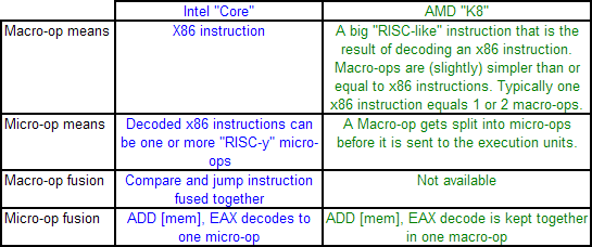
However, as mentioned above, AMD’s K8 has three complex decoders compared to Core’s 3 simple + 1 complex decoder arrangement. We also mentioned that simple decoders are smaller, use less power, and spit out one Intel micro-op per incoming variable length instruction. AMD K8 decoders on the other hand are dual purpose: it can implement Direct Path decoding, which is kind of like Intel’s simple decoder, or Vector decoding, which is kind of like Intel’s complex decoder. In almost all circumstances, the Direct Path is preferred as it produces fewer ops, and it turns out most instructions go down the Direct Path anyway, including floating point and SSE instructions in K8, resulting in fewer instructions over K7.
While extremely powerful in what they do, AMD’s limitation for K8, compared to Intel’s Core, is two-fold. AMD cannot perform Intel’s version of macro-op fusion, and so where Intel can pack one fused instruction to increase decode throughput such as the load and execute operations in SSE, AMD has to rely on two instructions. The next factor is that by virtue of having more decoders (4 vs 3), Intel can decode more per cycle, which expands with macro-op fusion – where Intel can decode five instructions per cycle, AMD is limited to just three.
As Johan pointed out in the original article, this makes it hard for AMD’s K8 to have had an advantage here. It would require three instructions to be fetched for the complex decoder on Intel, but not kick in the microcode sequencer. Since the most frequent x86 instructions map to one Intel micro-op, this situation is pretty unlikely.


158 Comments
View All Comments
Hazly79 - Wednesday, July 27, 2016 - link
History of Intel processori 386 1986
i 486 1989 - 94
Pentium / MMX 1994 - 96
Pentium II 1997
Pentium III 1999
Pentium 4 / 4 HT 2002 - 04
Pentium D 2005
Core [ 2 ] Duo 2006 - 08
Core [ 2 ] Quad 2007 - 08
Core [ i ] Nehalem 2008
Core [ i ] Westmere 2009
Core [ i ] Sandy Bridge 2011
Core [ i ] Ivy Bridge 2012
Core [ i ] Haswell 2013
Core [ i ] Broadwell 2014
Core [ i ] Skylake 2015
Core [ i ] Kabylake 2016
AnnonymousCoward - Wednesday, July 27, 2016 - link
So how many decades will it take til cpus have significantly faster single-thread than a 6700K@4.4GHz?Notmyusualid - Thursday, July 28, 2016 - link
+1Mr Perfect - Wednesday, July 27, 2016 - link
Hmm. We've got an ancient 2007 Macbook with a 2GHz C2D(T7200 I think) in it that's still used for web browsing on a daily basis. Upgrading it to 4GB of ram and a SSD made it surprisingly capable.It's not all a bed of roses though, as random things will come out of left field and floor it. I think it's mostly flash heavy sites, but Twitter and Vine freak it out a little.
Hulk - Wednesday, July 27, 2016 - link
I vividly remember the anticipation and hype leading up to the C2D release. The the years of struggle Intel had with Netburst before Conroe. It was what I consider the end of the golden age of the CPU. Great job Ian!Impulseman45 - Wednesday, July 27, 2016 - link
Ah, it wasn't the Pentium Pro it was based on. The Core family was a direct descendant of the Pentium 3 Tualatin. They stopped sales of the of the Pentium 3 Tualatin because it was outperforming the Pentium 4. They migrated that technology to the notebook line as it was much more efficient. It became the Pentium M. When Intel realized that the Pentium 4 Netburst architecture was a dead end and they needed a new chip to go up against AMD, they sourced their notebook chips to build the Core series. See this is what is called re-writing history. Come on guys, it is very well known that they sourced the Pentium M Yohan for the Core series. I do not know who did your research but it is all wrong. Go back and recheck your information. The Pentium Pro was the granddaddy of all the Pentium 2 and 3 chips so yeah, you can point to that chip in a vague way as the ancestor. But the Pentium 4 can as well well. So to be to the point, the core lines DNA goes back directly to the Pentium 3 Tualatin, So we have all been using very, very hopped up Pentium 3s the last 10 years. The Tualatin was an excellent chip. It overclock like crazy. There were Celeron and Sever P3 versions and all of them beat the hell out of the P4. Its know reason Intel had to kill it. Do more research so you can post accurate articles, please.Michael Bay - Thursday, July 28, 2016 - link
>teaching AT about CPU architecturesDamn it, you`re a riot!
Impulseman45 - Thursday, July 28, 2016 - link
These are not the original AT guys, they are all new people and they are not doing the research they should be doing. This is how history can get changed. People look to a reputable tech site that got something wrong and its written in stone. Well AT says this is how it is, even if they are wrong. Go check the history directly from Intel, This article is wrong and that is a fact, period. I felt it just needed to be called out on.natenu - Monday, August 1, 2016 - link
Refreshing to see this comment. HT was a marketing joke to keep up with clock rate shoppers.wumpus - Tuesday, August 2, 2016 - link
When Dave Barry jokes about "speed is measured in Megahertz" you know you are ripe for some marketing in your engineering.