The NVIDIA GeForce GTX 1080 Preview: A Look at What's to Come
by Ryan Smith on May 17, 2016 9:00 AM EST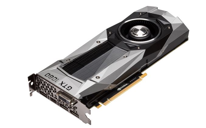
Earlier this month NVIDIA announced their latest generation flagship GeForce card, the GeForce GTX 1080. Based on their new Pascal architecture and built on TSMC’s 16nm FinFET process, the GTX 1080 is being launched as the first 16nm/14nm-based video card, and in time-honored fashion NVIDIA is starting at the high-end. The end result is that the GTX 1080 will be setting the new high mark for single-GPU performance.
Unlike past launches, NVIDIA is stretching out the launch of the GTX 1080 a bit more. After previously announcing it back on May 6th, the company is lifting their performance and architecture embargo today. Gamers however won’t be able to get their hands on the card until the 27th – next Friday – with pre-order sales starting this Friday. It is virtually guaranteed that the first batch of cards will sell out, but potential buyers will have a few days to mull over the data and decide if they want to throw down $699 for one of the first Founders Edition cards.
As for the AnandTech review, as I’ve only had a few days to work on the article, I’m going to hold it back rather than rush it out as a less thorough article. In the meantime however, as I know everyone is eager to see our take on performance, I wanted to take a quick look at the card and the numbers as a preview of what’s to come. Furthermore the entire performance dataset has been made available in the new GPU 2016 section of AnandTech Bench, for anyone who wants to see results at additional resolutions and settings.
Architecture
| NVIDIA GPU Specification Comparison | ||||||
| GTX 1080 | GTX 980 Ti | GTX 980 | GTX 780 | |||
| CUDA Cores | 2560 | 2816 | 2048 | 2304 | ||
| Texture Units | 160 | 176 | 128 | 192 | ||
| ROPs | 64 | 96 | 64 | 48 | ||
| Core Clock | 1607MHz | 1000MHz | 1126MHz | 863MHz | ||
| Boost Clock | 1733MHz | 1075MHz | 1216MHz | 900Mhz | ||
| TFLOPs (FMA) | 9 TFLOPs | 6 TFLOPs | 5 TFLOPs | 4.1 TFLOPs | ||
| Memory Clock | 10Gbps GDDR5X | 7Gbps GDDR5 | 7Gbps GDDR5 | 6Gbps GDDR5 | ||
| Memory Bus Width | 256-bit | 384-bit | 256-bit | 384-bit | ||
| VRAM | 8GB | 6GB | 4GB | 3GB | ||
| FP64 | 1/32 | 1/32 | 1/32 FP32 | 1/24 FP32 | ||
| TDP | 180W | 250W | 165W | 250W | ||
| GPU | GP104 | GM200 | GM204 | GK110 | ||
| Transistor Count | 7.2B | 8B | 5.2B | 7.1B | ||
| Manufacturing Process | TSMC 16nm | TSMC 28nm | TSMC 28nm | TSMC 28nm | ||
| Launch Date | 05/27/2016 | 06/01/2015 | 09/18/2014 | 05/23/2013 | ||
| Launch Price | MSRP: $599 Founders $699 |
$649 | $549 | $649 | ||
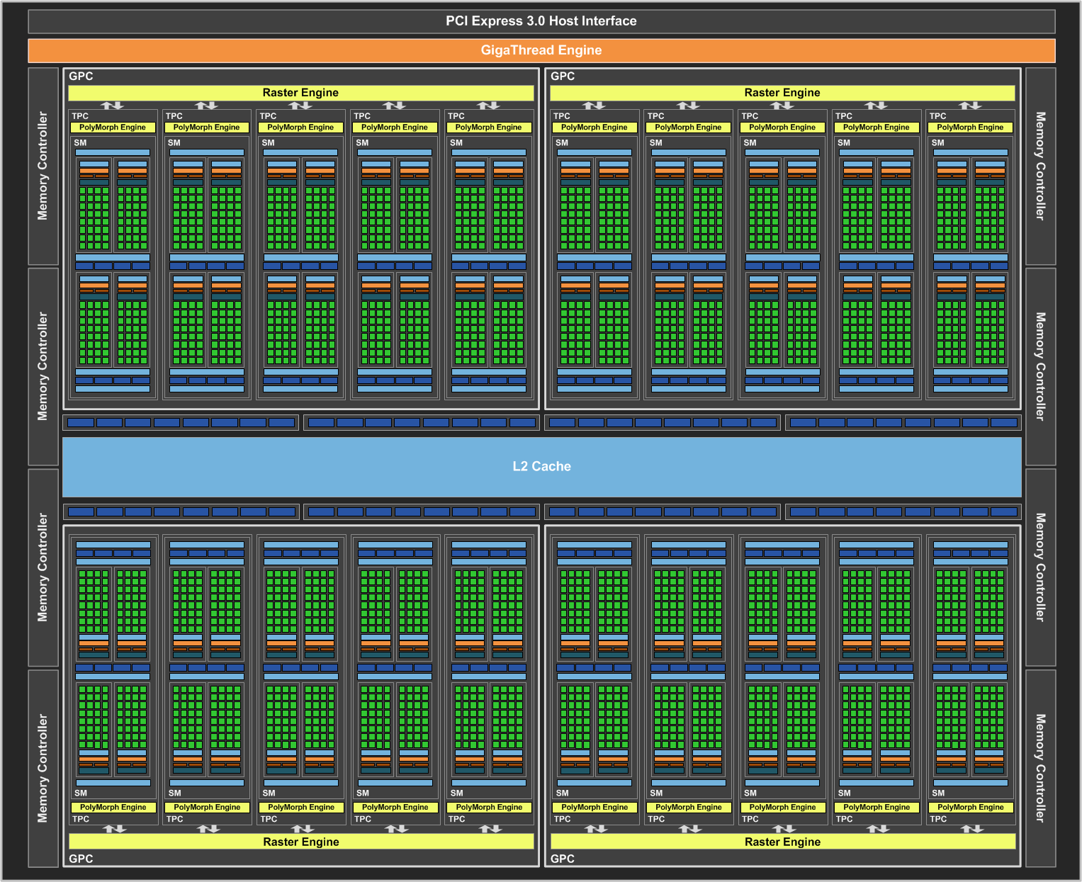
While I’ll get into architecture in much greater detail in the full article, at a high level the Pascal architecture (as implemented in GP104) is a mix of old and new; it’s not a revolution, but it’s an important refinement. Maxwell as an architecture was very successful for NVIDIA both at the consumer level and the professional level, and for the consumer iterations of Pascal, NVIDIA has not made any radical changes. The basic throughput of the architecture has not changed – the ALUs, texture units, ROPs, and caches all perform similar to how they did in GM2xx.
Consequently the performance aspects of consumer Pascal – we’ll ignore GP100 for the moment – are pretty easy to understand. NVIDIA’s focus on this generation has been on pouring on the clockspeed to push total compute throughput to 9 TFLOPs, and updating their memory subsystem to feed the beast that is GP104.
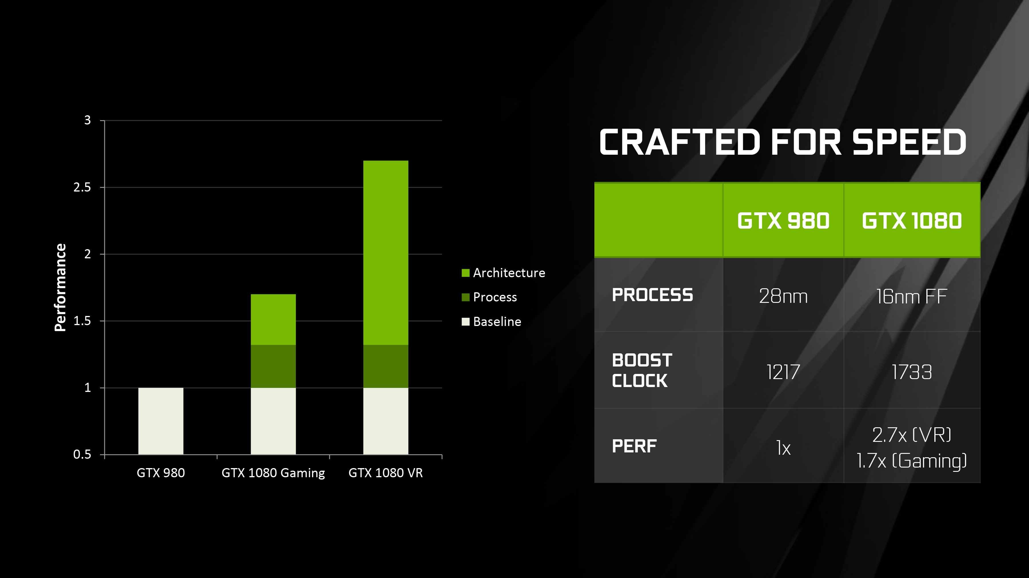
On the clockspeed front, a great deal of the gains come from the move to 16nm FinFET. The smaller process allows NVIDIA to design a 7.2B transistor chip at just 314mm2, while the use of FinFET transistors, though ultimately outright necessary for a process this small to avoid debilitating leakage, has a significant benefit to power consumption and the clockspeeds NVIDIA can get away with at practical levels of power consumption. To that end NVIDIA has sort of run with the idea of boosting clockspeeds, and relative to Maxwell they have done additional work at the chip design level to allow for higher clockspeeds at the necessary critical paths. All of this is coupled with energy efficiency optimizations at both the process and architectural level, in order to allow NVIDIA to hit these clockspeeds without blowing GTX 1080’s power budget.
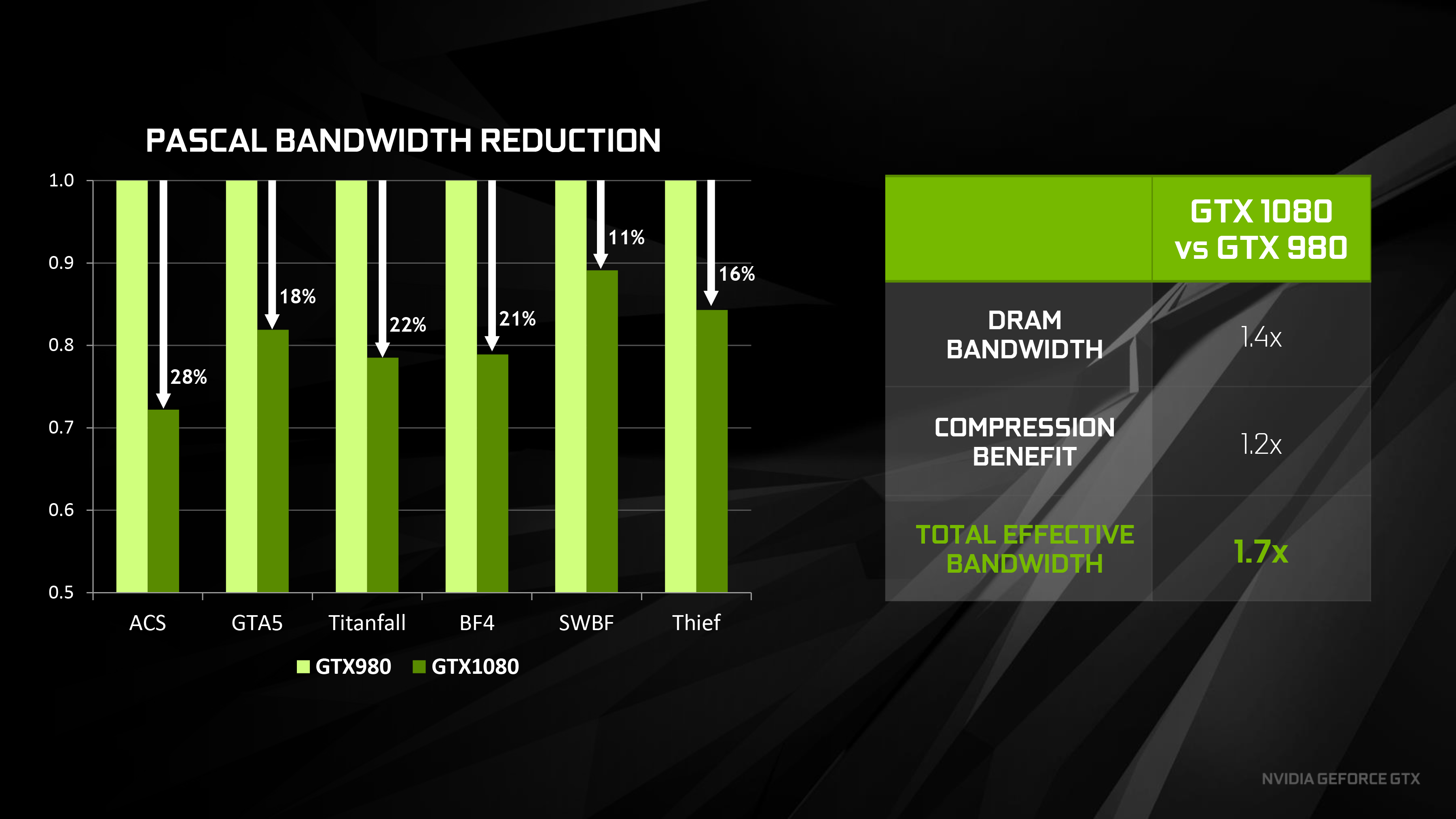
Meanwhile to feed GTX 1080, NVIDIA has made a pair of important changes to improve their effective memory bandwidth. The first of these is the inclusion of faster GDDR5X memory, which as implemented on GTX 1080 is capable of reaching 10Gb/sec/pin, a significant 43% jump in theoretical bandwidth over the 7Gb/sec/pin speeds offered by traditional GDDR5 on last-generation Maxwell products. Coupled with this is the latest iteration of NVIDIA’s delta color compression technology – now on its fourth generation – which sees NVIDIA once again expanding their pattern library to better compress frame buffers and render targets. NVIDIA’s figures put the effective memory bandwidth gain at 20%, or a roughly 17% reduction in memory bandwidth used thanks to the newer compression methods.
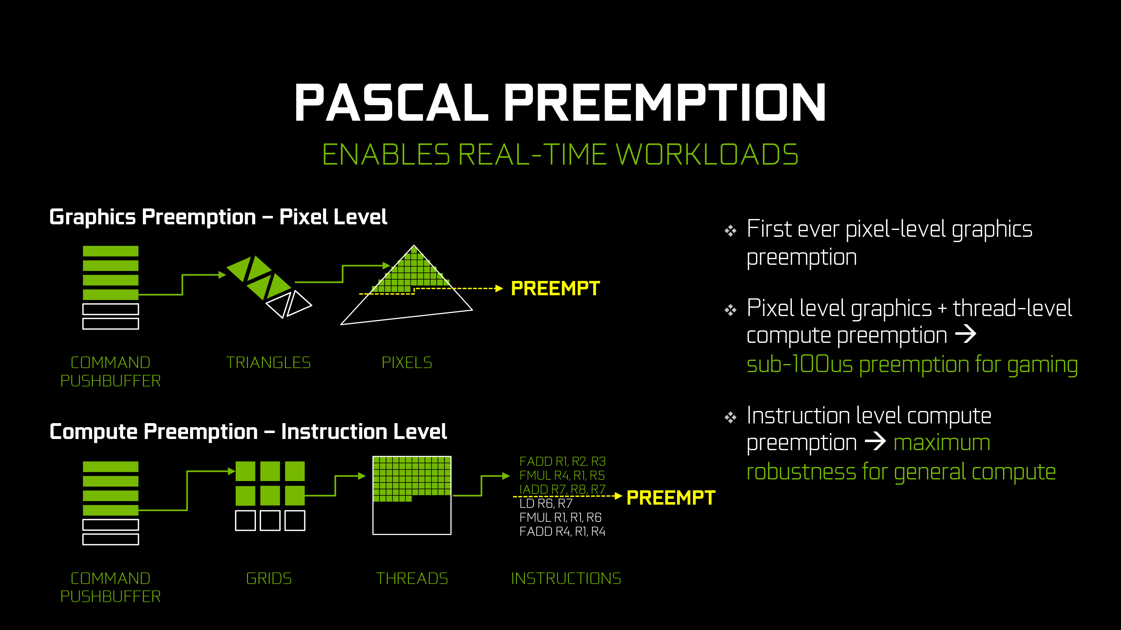
As for features included, we’ll touch upon that in a lot more detail in the full review. But while Pascal is not a massive overhaul of NVIDIA’s architecture, it’s not without its own feature additions. Pascal gains the ability to pre-empt graphics operations at the pixel (thread) level and compute operations at the instruction level, allowing for much faster context switching. And on the graphics side of matters, the architecture introduces a new geometry projection ability – Simultaneous Multi-Projection – and as a more minor update, gets bumped up to Conservative Rasterization Tier 2.
Looking at the raw specifications then, GTX 1080 does not disappoint. Though we’re looking at fewer CUDA cores than the GM200 based GTX 980 Ti or Titan, NVIDIA’s significant focus on clockspeed means that GP104’s 2560 CUDA cores are far more performant than a simple core count would suggest. The base clockspeed of 1607MHz is some 42% higher than GTX 980 (and 60% higher than GTX 980 Ti), and the 1733MHz boost clockspeed is a similar gain. On paper, GTX 1080 is set to offer 78% better performance than GTX 980, and 47% better performance than GTX 980 Ti. The real world gains are, of course, not quite this great, but they’re also relatively close to these numbers at times.


262 Comments
View All Comments
Yojimbo - Thursday, May 19, 2016 - link
Why is everything 100% with you? Neither of us know 100% anything about this issue. And the fact that half precision at double throughput is not possible on the GTX 1080 does not mean that it's not possible on the GP104.Further explanation of what you said "huh?" to: NVIDIA revealed the Drive PX 2 at both CES 2016 and GTC 2016. It has two Pascal-based Tegra chips and two larger Pascal GPUs. The main purpose of the Drive PX 2 will be to run inference algorithms for self driving cars. There are large portions of these algorithms which only require FP16 precision. NVIDIA would be leaving performance on the table if they didn't include the FP16 throughput enhancements in whatever chips they are using for the Drive PX 2. And those GPUs are definitely not GP100s. Unless they specially designed another GPU that is based on the GP100, but much smaller, they are probably using something along the lines of a GP106 or GP107 for that purpose.
I'm guessing it's easier to design 6 GPUs and put FP16 enhancements in all of them then it is to design 8 GPUs and put FP16 enhancements in 4 of them. I don't think you have any reason to believe it's so difficult for them to put the FP16 enhancements into GP104. (They had already done so for the Maxwell-based Tegra X1, by the way.) You just seem to want to believe things which fit into your preferred narrative of "GTX 1080 is almost identical to Maxwell".
dragonsqrrl - Wednesday, May 18, 2016 - link
@vladxThey're all based on the same underlying architecture (Pascal). I'm actually not sure why you think GP104 is closer to Maxwell architecturally than GP100. Are you referring to the SMM layout?
Ryan Smith - Wednesday, May 18, 2016 - link
"Does it support the special instructions that the Tesla P100 has for half precision float (FP16), which double throughput?"The answer is basically no. More info to come in the full review.
modeless - Thursday, May 19, 2016 - link
:( Thanks. Hope NVIDIA gets some competition in deep learning soon...Yojimbo - Thursday, May 19, 2016 - link
They have competition already with Xeon Phi and CPUs. The trouble with AMD's GPUs for deep learning is that they don't have nearly the same level of library support as NVIDIA's GPUs do. Intel is also hoping to adapt FPGAs for deep learning purposes, I think, but I doubt that's going to help you out much.damianrobertjones - Tuesday, May 17, 2016 - link
Each new gen sees around an extra 10/14fps being added to the top card over the previous gen. No. No thank you. These companies keep DRIP FEEDING us small advances and, obviously, this is business.Spend your cash, fine, but they're laughing at us each time. (I have an ebay 980)
FMinus - Tuesday, May 17, 2016 - link
Though the move was from Maxwell to Pascal, looks more like Paxwell, Maxwell on steroids - 70% clock, 30% compression, not much innovation. And that PCB is a disgrace, skimping on the 6th phase, and only one mosfet per VRM phase - weren't they speaking of premium components thus the added premium, certainly doesn't look premium.leoneo.x64 - Tuesday, May 17, 2016 - link
Ryan. Please excuse me for asking. I am not being rude. But where is part 2 of the Galaxy s7 edge review?leoneo.x64 - Tuesday, May 17, 2016 - link
Ryan. Please excuse me for asking. I am not being rude. But where is part 2 of the Galaxy s7 edge review?Lolimaster - Tuesday, May 17, 2016 - link
Fail gen for nvidia.They need 1.7Ghz to actually show improvement vs the 1-1.2Ghz of the previous AMD/Nvidia gpu's. Imagine the GP104 at 1.2Ghz.
Wheres the efficiency?
Polaris 10 is aiming at the same 1Ghz sweet spot, improving the hell out of it's gpu cores.