The NVIDIA GeForce GTX 1080 & GTX 1070 Founders Editions Review: Kicking Off the FinFET Generation
by Ryan Smith on July 20, 2016 8:45 AM ESTGP104: The Heart of GTX 1080
At the heart of the GTX 1080 is the first of the consumer-focused Pascal GPUs, GP104. Though no two GPU generations are ever quite alike, GP104 follows a number of design cues established with the past couple 104 GPUs. Overall 104 GPUs have struck a balance between size and performance, allowing NVIDIA to get a suitably high yielding GPU out at the start of a generation, and to be followed up with larger GPUs later on as yields improve. With the exception of the GTX 780, 104 GPUs been the backbone of NVIDIA’s GTX 70 and 80 parts, and that is once again the case for the Pascal generation.
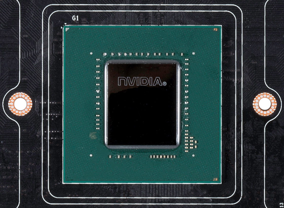
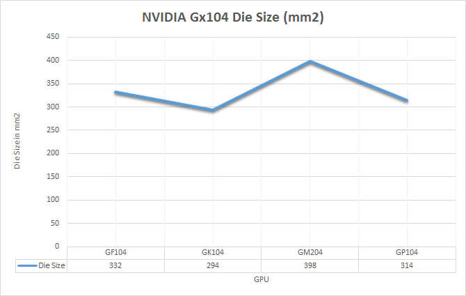
In terms of die size, GP104 comes in at 314mm2. This is right in NVIDIA’s traditional sweet spot for these designs, slotting in between the 294mm2 GK104 and the 332mm2 GF104. In terms of total transistors we’re looking at 7.2B transistors, up from 3.5B on GK104 and the 5.2B of the more unusual GM204. The significant increase in density comes from the use of TSMC’s 16nm FinFET process, which compared to 28nm combines a full node shrink, something that has been harder and harder to come by as the years have progressed.
Though the density improvement offered by TSMC’s 16nm process is of great importance to GP104’s overall performance, for once density takes a back seat to the properties of the process itself. I am of course speaking about the FinFET transistors, which are the headlining feature of TSMC’s process.
We’ve covered FinFET technology in depth before, so I won’t completely rehash it here. But in brief, FinFETs are an important development for chip fabrication as processes have gone below 28nm. As traditional, planar transistors have shrunk in feature size – and ultimately, the number of atoms they’re comprised of – electrical leakage has increased. With fewer atoms in a transistor, there are equally fewer atoms to control the flow of electrons.
FinFET in turn is a solution to this problem, essentially allowing fabs to turn back the clock on electrical leakage. By building transistors as three-dimensional objects with height as opposed to two-dimensional objects, giving FinFET transistors their characteristic fins in the process, FinFET technology greatly reduces the amount of energy a transistor leaks. In practice what this means is that FinFET technology not only reduces the total amount of energy wasted from leakage, but it also allows transistors to be operated at a much lower voltage, something we’ll see in depth with our analysis of GTX 1080.
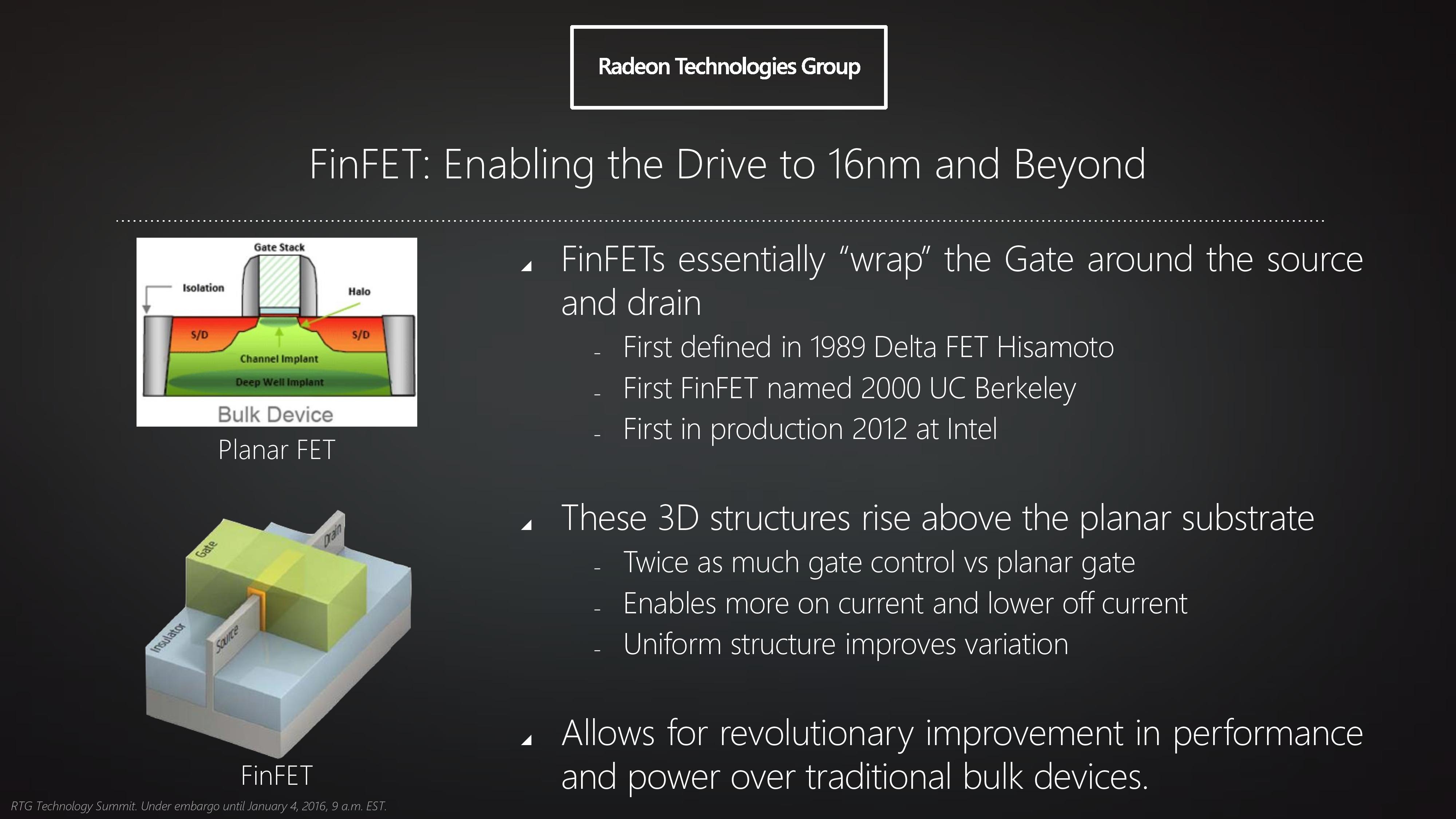
FinFETs, or rather the lack thereof, are a big part of why we never saw GPUs built on TSMC’s 20nm process. It was TSMC’s initial belief that they could contain leakage well enough using traditional High-K Metal Gate (HKMG) technology on 20nm, a bet they ultimately lost. At 20nm, planar transistors were just too leaky to use for many applications, which is why ultimately we only saw SoCs on 20nm (and even then they were suboptimal). FinFETs, as it turns out, are absolutely necessary to get good performance out of transistors built on processes below 28nm.
And while it took TSMC some time to get there, now that they have the capability NVIDIA can reap the benefits. Not only can NVIDIA finally build a relatively massive chip like a GPU on a sub-28nm process, but thanks to the various beneficial properties of FinFETs, it allows them to take their designs in a different direction than what they could do on 28nm.


200 Comments
View All Comments
patrickjp93 - Wednesday, July 20, 2016 - link
That doesn't actually support your point...Scali - Wednesday, July 20, 2016 - link
Did I read a different article?Because the article that I read said that the 'holes' would be pretty similar on Maxwell v2 and Pascal, given that they have very similar architectures. However, Pascal is more efficient at filling the holes with its dynamic repartitioning.
mr.techguru - Wednesday, July 20, 2016 - link
Just Ordered the MSI GeForce GTX 1070 Gaming X , way better than 1060 / 480. NVidia Nail it :)tipoo - Wednesday, July 20, 2016 - link
" NVIDIA tells us that it can be done in under 100us (0.1ms), or about 170,000 clock cycles."Is my understanding right that Polaris, and I think even earlier with late GCN parts, could seamlessly interleave per-clock? So 170,000 times faster than Pascal in clock cycles (less in total time, but still above 100,000 times faster)?
Scali - Wednesday, July 20, 2016 - link
That seems highly unlikely. Switching to another task is going to take some time, because you also need to switch all the registers, buffers, caches need to be re-filled etc.The only way to avoid most of that is to duplicate the whole register file, like HyperThreading does. That's doable on an x86 CPU, but a GPU has way more registers.
Besides, as we can see, nVidia's approach is fast enough in practice. Why throw tons of silicon on making context switching faster than it needs to be? You want to avoid context switches as much as possible anyway.
Sadly AMD doesn't seem to go into any detail, but I'm pretty sure it's going to be in the same ballpark.
My guess is that what AMD calls an 'ACE' is actually very similar to the SMs and their command queues on the Pascal side.
Ryan Smith - Wednesday, July 20, 2016 - link
Task switching is separate from interleaving. Interleaving takes place on all GPUs as a basic form of latency hiding (GPUs are very high latency).The big difference is that interleaving uses different threads from the same task; task switching by its very nature loads up another task entirely.
Scali - Thursday, July 21, 2016 - link
After re-reading AMD's asynchronous shader PDF, it seems that AMD also speaks of 'interleaving' when they switch a graphics CU to a compute task after the graphics task has completed. So 'interleaving' at task level, rather than at instruction level.Which would be pretty much the same as NVidia's Dynamic Load Balancing in Pascal.
eddman - Thursday, July 21, 2016 - link
The more I read about async computing in Polaris and Pascal, the more I realize that the implementations are not much different.As Ryan pointed out, it seems that the reason that Polaris, and GCN as a whole, benefit more from async is the architecture of the GPU itself, being wider and having more ALUs.
Nonetheless, I'm sure we're still going to see comments like "Polaris does async in hardware. Pascal is hopeless with its software async hack".
Matt Doyle - Wednesday, July 20, 2016 - link
Typo in the lead sentence of HPC vs. Consumer: Divergence paragraph: "Pascal in an architecture that...""is" instead of "in"
Matt Doyle - Wednesday, July 20, 2016 - link
Feeding Pascal page, "GDDR5X uses a 16n prefetch, which is twice the size of GDDR5’s 8n prefect."Prefect = prefetch