The NVIDIA GeForce GTX 1080 & GTX 1070 Founders Editions Review: Kicking Off the FinFET Generation
by Ryan Smith on July 20, 2016 8:45 AM ESTGPU Boost 3.0: Finer-Grained Clockspeed Controls
While much of this is abstracted away in everyday GPU discussions, under the hood the concept of clockspeed is a little lot more complex than the simple base clock and boost clock numbers posted in specification tables. Since the introduction of Kepler, NVIDIA has introduced fine-grained voltage points, which defines a series of GPU voltages and their respective clockspeeds. The GPU in turn operates at points along the resulting curve, shifting clockspeeds based on which voltage it’s at and what the environmental conditions are.
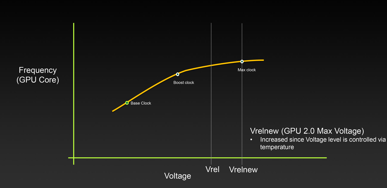
While these voltage points have been present since Kepler, NVIDIA has not, until now, exposed them to end users. However with Pascal this is finally changing, with the introduction of GPU Boost 3.0.
With the latest rendition of NVIDIA’s GPU clockspeed management technology, NVIDIA has made the individual voltage points programmable, and in turn they are exposing this functionality to third party overclocking programs via NVAPI. Consequently it is now possible to adjust the clockspeed of Pascal GPUs at each voltage point, a much greater level of control than before.
The addition of finer-grained controls is designed to improve the flexibility of overclocking on Pascal. Prior to GPU Boost 3.0, the only way to overclock was to adjust the clockspeed for all voltage points by the same amount at the same time – or in NVIDIA’s GPU Boost 3.0 vernacular, a fixed frequency offset. While this certainly works, it limits the highest stable overclock to the lowest point on the voltage/frequency curve. If the GPU can only overclock by 50MHz at the highest voltage point, but 100MHz at a middle point, then the highest stable overclock is only going to be 50MHz.
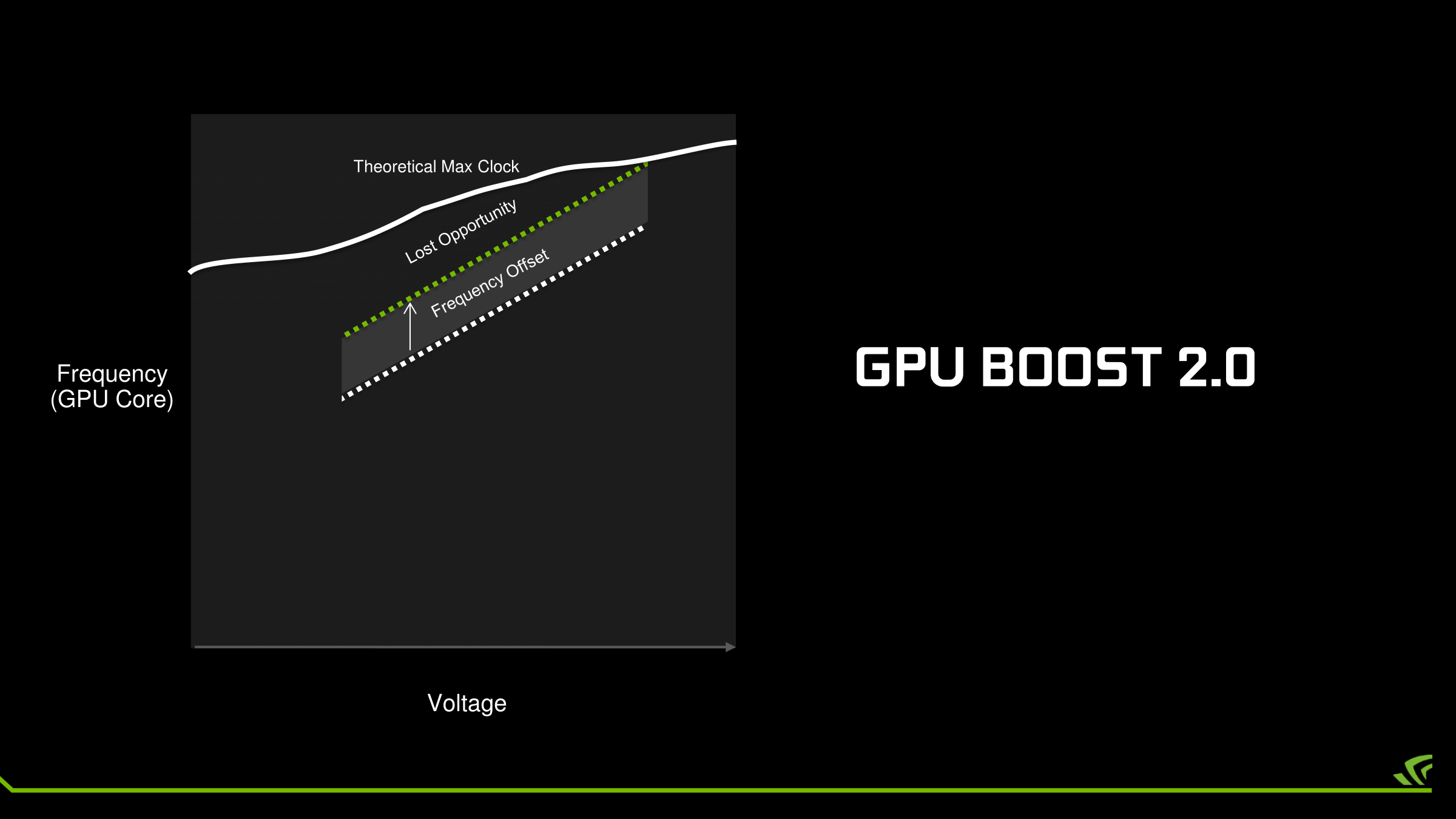
With GPU Boost 3.0 on the other hand, each point on the curve can be adjusted individually. This means the weakest points can be overclocked to a lesser degree while the strongest points can be more significantly overclocked. All other things held equal, this should improve GPU overclocking performance, as GPU tends to shift along multiple points when it’s running. Put another way: GPU Boost 3.0 seeks to wring out the last bits of overclocking headroom along the voltage frequency curve. The only way to go higher still would be to increase the voltage, which NVIDIA hasn’t truly allowed since Fermi.
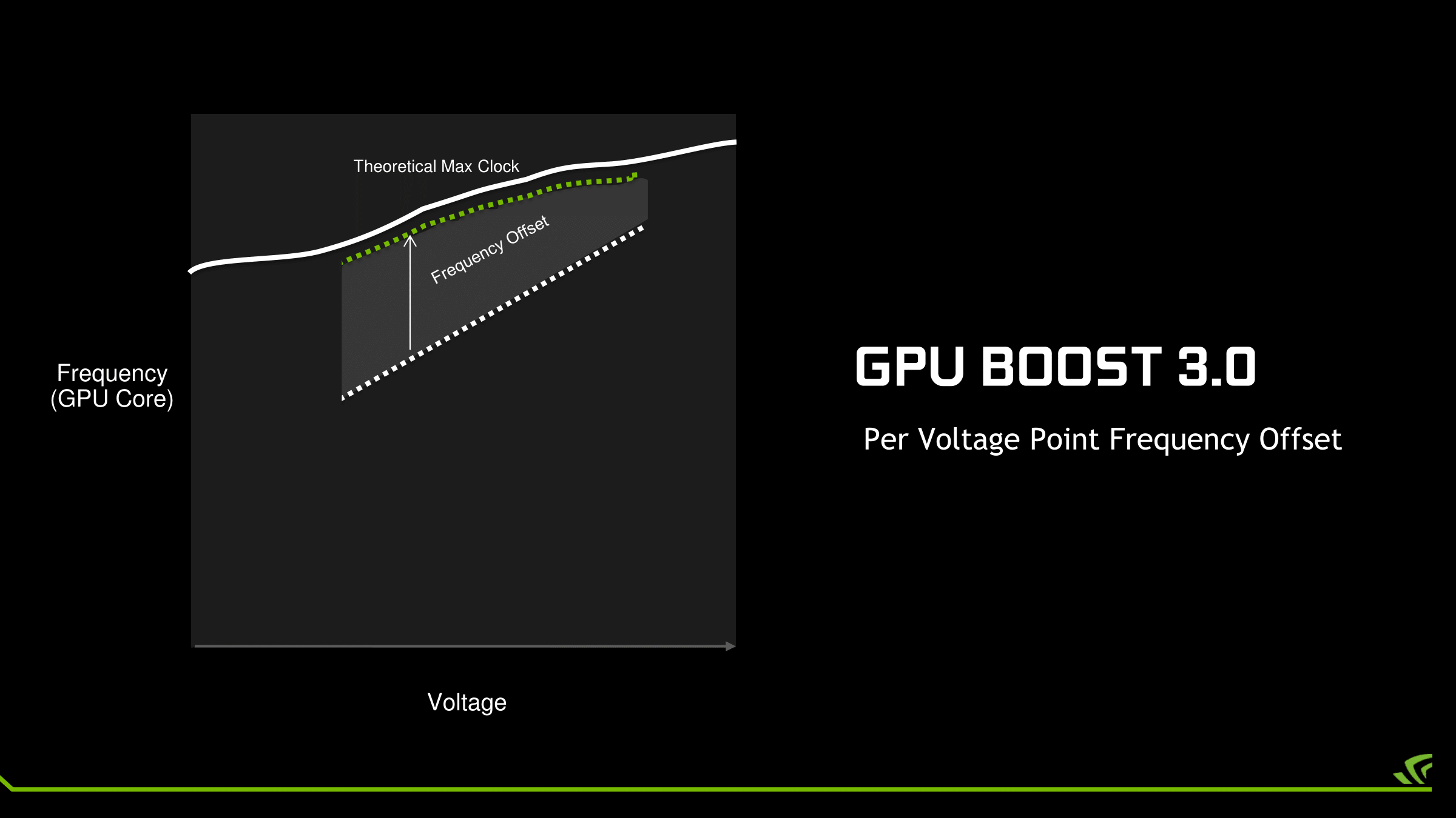
Meanwhile, the flip side of having finer-grained controls is that it’s now more work to dial in the perfect overclock. Rather than testing one overclock you now have to test nearly two-dozen voltage points to fully exploit GPU Boost 3.0’s abilities, which is time consuming at the best of times. As a result NVIDIA has also exposed a setting in NVAPI to lock the GPU at a specific voltage point. The significance of this is that it now allows overclocking utilities to go through the voltage points and discretely test each one.
The first software to implement this concept is EVGA’s Precision XOC. The latest iteration of EVGA’s overclocking software is able to go through the voltage points and run an OC ScannerX test on each one to find its stability. When a point fails, Precision XOC will then back off the frequency at that point and move on. The end result is that after a series of trials and failures, you should have the virtually-perfect overclock.
Unfortunately while this is sound in concept, in practice NVIDIA and EVGA still aren’t quite there yet. Overclocking failures can cause multiple types of failures; graphic corruption (easy to catch and recover), driver crashes (moderately difficult to recover from), and system hardlocks (very difficult to recover from). In practice, Precision XOC isn’t yet at the point where it can quickly and efficiently handle the last two cases; so driver crashes and system hardlocks still require human intervention, and Precision XOC doesn’t do a great job of resuming from where it left off.
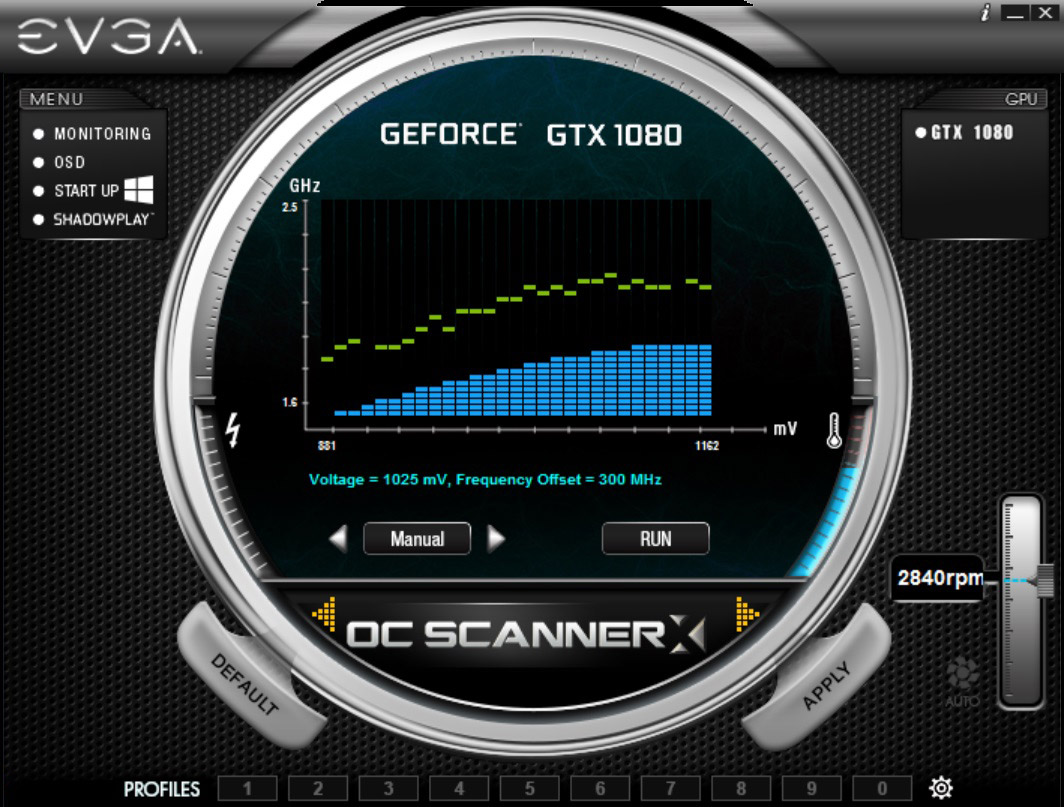
Hopefully one day NVIDIA and EVGA will get there, but for now the only practical way to fully exploit GPU Boost 3.0 is the tedious way. This means either using traditional offset overclocking, or a mode NVIDIA calls linear overclocking, in which the slope of the voltage/frequency curve is adjusted rather than offset (think m in y=mx+b rather than b). In this case two points are picked, and all of the voltage points are overclocked to match the resulting linear curve.
Observations on Clocking with Pascal
While we’re on the subject of clockspeed management on Pascal, I want to discuss my observations with how clockspeeds work on NVIDIA’s newest GPU. When it comes to clockspeed management NVIDIA hasn’t just changed how overclocking works, but relative to Kepler/Maxwell, there are some other, subtle changes.
To start, Pascal clockspeeds are much more temperature-dependent than on Maxwell 2 or Kepler. Kepler would drop a single bin at a specific temperature, and Maxwell 2 would sustain the same clockspeed throughout. However Pascal will drop its clockspeeds as the GPU warms up, regardless of whether it still has formal thermal and TDP headroom to spare. This happens by backing off both on the clockspeed at each individual voltage point, and backing off to lower voltage points altogether.
To quantify this effect, I ran LuxMark 3.1 continuously for several minutes, until the GPU temperature leveled out. As a compute test, LuxMark does not cause the GTX 1080 to hit its 83C temperature limit nor its 180W TDP limit, so it’s a good example of the temperature compensation effect.
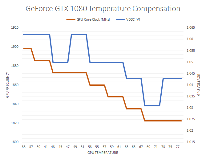
What we find is that from the start of the run until the end, the GPU clockspeed drops from the maximum boost bin of 1898MHz to a sustained 1822MHz, a drop of 4%, or 6 clockspeed bins. These shifts happen relatively consistently up to 68C, after which they stop.
For what it’s worth, the GTX 1080 gets up to 68C relatively quickly, so GPU performance stabilizes rather soon. But this does mean that GTX 1080’s performance is more temperature dependent than GTX 980’s. Throwing a GTX 1080 under water could very well net you a few percent performance increase by avoiding the compensation effect, along with any performance gained from avoiding the card’s 83C temperature throttle.
In any case, I believe this to be compensation for the effects of higher temperatures on the GPU, backing off on voltages/clockspeeds due to potential issues. What those issues are I’m not sure; it could be that 16nm FinFET doesn’t like high voltages at higher temperatures (NVIDIA takes several steps to minimize GPU degradation), or something else entirely.
Otherwise, outside of the temperature compensation effect, clockspeeds on GTX 1080 appear to mostly be a function of temperature or running out of boost bins (VREL limited). The card rarely appears to be TDP limited, especially at steady-state. This indicates that NVIDIA could probably increase the fan speed of the cooler a bit to get a bit more performance, but at the cost of generating a bit more noise.
Finally, how overvolting is being represented is a bit different from before. Previously NVIDIA (and EVGA Precision) would show the exact additional voltage (i.e. the voltage of the unlocked voltage points) when overvolting. However now overvolting is expressed on a percentage scale from 0% to 100%, which obfuscates what the higher voltage points actually are. However this hasn’t changed the underlying behavior of overvolting; one or more voltage points are calibrated by NVIDIA, but they are locked due to the potential for GPU degradation. Overvolting then unlocks these points, allowing the GPU to boost higher so long as there is thermal and power headroom to allow it.


200 Comments
View All Comments
grrrgrrr - Wednesday, July 20, 2016 - link
Solid review! Some nice architecture introductions.euskalzabe - Wednesday, July 20, 2016 - link
The HDR discussion of this review was super interesting, but as always, there's one key piece of information missing: WHEN are we going to see HDR monitors that take advantage of these new GPU abilities?I myself am stuck at 1080p IPS because more resolution doesn't entice me, and there's nothing better than IPS. I'm waiting for HDR to buy my next monitor, but being 5 years old my Dell ST2220T is getting long in the teeth...
ajlueke - Wednesday, July 20, 2016 - link
Thanks for the review Ryan,I think the results are quite interesting, and the games chosen really help show the advantages and limitations of the different architectures. When you compare the GTX 1080 to its price predecessor, the 980 Ti, you are getting an almost universal ~25%-30% increase in performance.
Against rival AMDs R9 Fury X, there is more of a mixed bag. As the resolutions increase the bandwidth provided by the HBM memory on the Fury X really narrows the gap, sometimes trimming the margin to less that 10%,s specifically in games optimized more for DX12 "Hitman, "AotS". But it other games, specifically "Rise of the Tomb Raider" which boasts extremely high res textures, the 4Gb memory size on the Fury X starts to limit its performance in a big way. On average, there is again a ~25%-30% performance increase with much higher game to game variability.
This data lets a little bit of air out of the argument I hear a lot that AMD makes more "future proof" cards. While many Nvidia 900 series users may have to upgrade as more and more games switch to DX12 based programming. AMD Fury users will be in the same boat as those same games come with higher and higher res textures, due to the smaller amount of memory on board.
While Pascal still doesn't show the jump in DX12 versus DX11 that AMD's GPUs enjoy, it does at least show an increase or at least remain at parity.
So what you have is a card that wins in every single game tested, at every resolution over the price predecessors from both companies, all while consuming less power. That is a win pretty much any way you slice it. But there are elements of Nvidia’s strategy and the card I personally find disappointing.
I understand Nvidia wants to keep features specific to the higher margin professional cards, but avoiding HBM2 altogether in the consumer space seems to be a missed opportunity. I am a huge fan of the mini ITX gaming machines. And the Fury Nano, at the $450 price point is a great card. With an NVMe motherboard and NAS storage the need for drive bays in the case is eliminated, the Fury Nano at only 6” leads to some great forward thinking, and tiny designs. I was hoping to see an explosion of cases that cut out the need for supporting 10-11” cards and tons of drive bays if both Nvidia and AMD put out GPUs in the Nano space, but it seems not to be. HBM2 seems destined to remain on professional cards, as Nvidia won’t take the risk of adding it to a consumer Titan or GTX 1080 Ti card and potentially again cannibalize the higher margin professional card market. Now case makers don’t really have the same incentive to build smaller cases if the Fury Nano will still be the only card at that size. It’s just unfortunate that it had to happen because NVidia decided HBM2 was something they could slap on a pro card and sell for thousands extra.
But also what is also disappointing about Pascal stems from the GTX 1080 vs GTX 1070 data Ryan has shown. The GTX 1070 drops off far more than one would expect based off CUDA core numbers as the resolution increases. The GDDR5 memory versus the GDDR5X is probably at fault here, leading me to believe that Pascal can gain even further if the memory bandwidth is increased more, again with HBM2. So not only does the card limit you to the current mini-ITX monstrosities (I’m looking at you bulldog) by avoiding HBM2, it also very likely is costing us performance.
Now for the rank speculation. The data does present some interesting scenarios for the future. With the Fury X able to approach the GTX 1080 at high resolutions, most specifically in DX12 optimized games. It seems extremely likely that the Vega GPU will be able to surpass the GTX 1080, especially if the greatest limitation (4 Gb HBM) is removed with the supposed 8Gb of HBM2 and games move more and more the DX12. I imagine when it launches it will be the 4K card to get, as the Fury X already acquits itself very well there. For me personally, I will have to wait for the Vega Nano to realize my Mini-ITX dreams, unless of course, AMD doesn’t make another Nano edition card and the dream is dead. A possibility I dare not think about.
eddman - Wednesday, July 20, 2016 - link
The gap getting narrower at higher resolutions probably has more to do with chips' designs rather than bandwidth. After all, Fury is the big GCN chip optimized for high resolutions. Even though GP104 does well, it's still the middle Pascal chip.P.S. Please separate the paragraphs. It's a pain, reading your comment.
Eidigean - Wednesday, July 20, 2016 - link
The GTX 1070 is really just a way for Nvidia to sell GP104's that didn't pass all of their tests. Don't expect them to put expensive memory on a card where they're only looking to make their money back. Keeping the card cost down, hoping it sells, is more important to them.If there's a defect anywhere within one of the GPC's, the entire GPC is disabled and the chip is sold at a discount instead of being thrown out. I would not buy a 1070 which is really just a crippled 1080.
I'll be buying a 1080 for my 2560x1600 desktop, and an EVGA 1060 for my Mini-ITX build; which has a limited power supply.
mikael.skytter - Wednesday, July 20, 2016 - link
Thanks Ryan! Much appreciated.chrisp_6@yahoo.com - Wednesday, July 20, 2016 - link
Very good review. One minor comment to the article writers - do a final check on grammer - granted we are technical folks, but it was noticeable especially on the final words page.madwolfa - Wednesday, July 20, 2016 - link
It's "grammar", though. :)Eden-K121D - Thursday, July 21, 2016 - link
Oh the ironychrisp_6@yahoo.com - Thursday, July 21, 2016 - link
oh snap, that is some funny stuff right there