NVIDIA Announces the GeForce GTX 1000 Series: GTX 1080 and GTX 1070 Arrive In May & June
by Ryan Smith on May 7, 2016 3:25 AM ESTGeForce GTX 1080
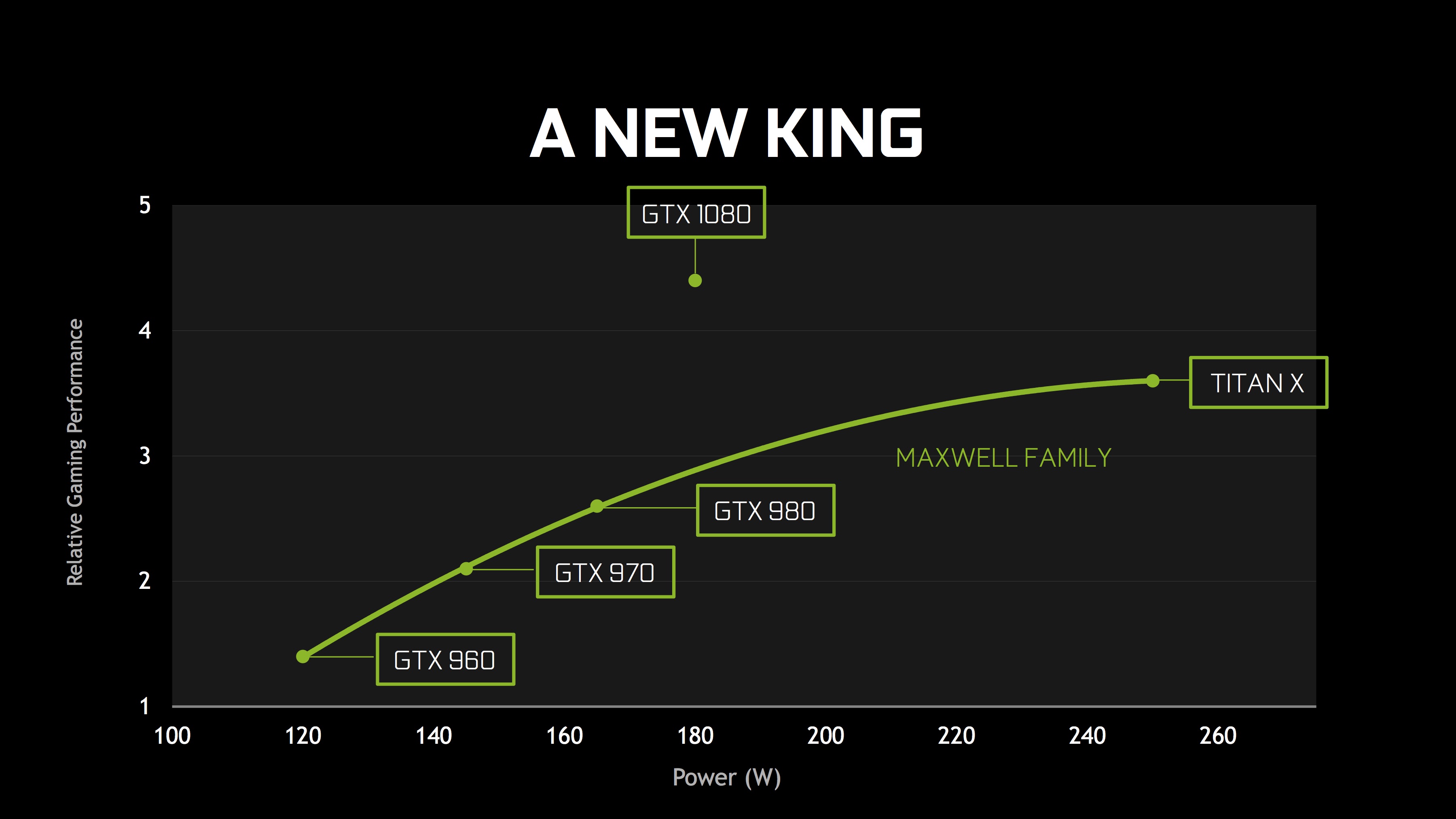
With Pascal/GP104 particulars out of the way, let’s talk about the cards themselves. “The new king” as NVIDIA affectionately calls it will be the GTX 1080, and will be their new flagship card. NVIDIA is promoting it as having better performance than both GTX 980 SLI and GTX Titan X. NVIDIA’s own performance marketing slides put the average at around 65% faster than GTX 980 and 20-25% faster than GTX Titan X/980 Ti, which is relatively consistent for a new NVIDIA GPU. Of course, real-world performance remains to be seen, and will vary from game to game.
| NVIDIA GTX x80 Specification Comparison | ||||||
| GTX 1080 | GTX 1070 | GTX 980 | GTX 780 | |||
| CUDA Cores | 2560 | (Fewer) | 2048 | 2304 | ||
| Texture Units | 160? | (How many?) | 128 | 192 | ||
| ROPs | 64 | (Good question) | 64 | 48 | ||
| Core Clock | 1607MHz | (Slower) | 1126MHz | 863MHz | ||
| Boost Clock | 1733MHz | (Again) | 1216MHz | 900Mhz | ||
| TFLOPs (FMA) | 9 TFLOPs | 6.5 TFLOPs | 5 TFLOPs | 4.1 TFLOPs | ||
| Memory Clock | 10Gbps GDDR5X | GDDR5 | 7Gbps GDDR5 | 6Gbps GDDR5 | ||
| Memory Bus Width | 256-bit | ? | 256-bit | 256-bit | ||
| VRAM | 8GB | 8GB | 4GB | 3GB | ||
| FP64 | ? | ? | 1/32 FP32 | 1/24 FP32 | ||
| TDP | 180W | ? | 165W | 250W | ||
| GPU | "GP104" | "GP104" | GM204 | GK110 | ||
| Transistor Count | 7.2B | 7.2B | 5.2B | 7.1B | ||
| Manufacturing Process | TSMC 16nm | TSMC 16nm | TSMC 28nm | TSMC 28nm | ||
| Launch Date | 05/27/2016 | 06/10/2016 | 09/18/2014 | 05/23/2013 | ||
| Launch Price | MSRP: $599 Founders $699 |
MSRP:$379 Founders: $449 |
$549 | $649 | ||
The GTX 1080 will ship with the most powerful GP104 implementation – we don’t yet have confirmation of whether it’s fully enabled – with 2560 of Pascal’s higher efficiency CUDA cores. And while I’m also awaiting confirmation of this as well, I believe it’s a very safe bet that the card will feature 160 texture units and 64 ROPs, given what is known about the architecture.
Along with Pascal’s architectural efficiency gains, the other big contributor to GTX 1080’s performance will come from its high clockspeed. The card will ship with a base clock of 1607MHz and a boost clock of 1733MHz. This is a significant 43% boost in operating frequency over GTX 980, and it will be interesting to hear how much of this is from the jump to 16nm and how much of this is from any kind of specific optimization to hit higher clockspeeds. Meanwhile NVIDIA is touting that GTX 1080 will be a solid overclocker, demoing it running at 2114MHz with its reference air cooler in their presentation.
GTX 1080 will be paired with 8GB of the new GDDR5X memory, on a 256-bit memory bus. The shift to GDDR5X allows NVIDIA to run GTX 1080 at 10Gbps/pin, giving the card a total of 320GB/sec of memory bandwidth. Interestingly, even with GDDRX5 this is still a bit less memory bandwidth than GTX 980 Ti (336GB/sec), a reminder that even with GDDR5X, memory bandwidth improvements continue to be outpaced by GPU throughput improvements, so memory bandwidth efficiency is always paramount.
I am admittedly a bit surprised that GTX 1080’s GDDR5X is only clocked at 10Gbps, and not something faster. Micron’s current chips are rated for up to 12Gbps, and the standard itself is meant to go up to 14Gbps. So I am curious over whether this is NVIDIA holding back so that they have some future headroom, whether this is a chip supply thing, or if perhaps GP104 simply can’t do 12Gbps at this time. At the same time it will be interesting to see whether the fact that NVIDIA can currently only source GDDRX from a single supplier (Micron) has any impact, as GDDR5 was always multi-sourced. Micron for their part has previously announced that their GDDR5X production line wouldn’t reach volume production until the summer, which is a potential indicator that GDDR5X supplies will be limited.
On the power front, NVIDIA has given the GTX 1080 an 180W TDP rating. This is 15W higher than the GTX 980, so the GTX x80 line is drifting back up a bit in TDP, but overall NVIDIA is still trying to keep the GTX x80 lineup as mid-power cards, as this worked well for them with GTX 680/980. Meanwhile thanks to Pascal and 16nm this is much lower than GTX 980 Ti for higher performance. We’ll look at card design a bit more in a moment, but I do want to note that NVIDIA is using a single 8-pin PCIe power connector for this, as opposed to 2 6-pin connectors, and this is something that is becoming increasingly common.

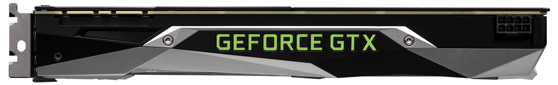
Looking at the design of the card itself, the GTX 1080 retains a lot of the signature style of NVIDIA’s other high-end reference cards, however after using the same industrial design since the original GTX Titan in 2013, NVIDIA has rolled out a new industrial design for the GTX 1000 series. The new design is far more (tri)angular as opposed to the squared-off GTX Titan cooler. Otherwise limited information is available about this design and whether the change improves cooling/noise in some fashion, or if this is part of NVIDIA’s overall fascination with triangles. Though one thing that has not changed is size: this is a 10.5” double-wide card, the same as all of the cards that used the previous design.
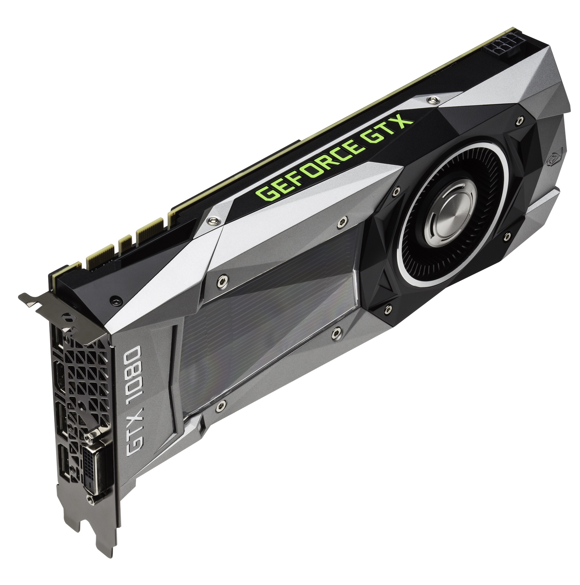
Industrial design aside, NVIDIA confirmed that the GTX 1080 will come with a vapor chamber cooler; GTX 980 did not do this, as NVIDIA didn’t believe this was necessary on a 165W card. Given NVIDIA’s overclocking promises with this card, this likely has something to do with it, as a vapor chamber should prove very capable on a 180W card.

Meanwhile it looks like the DVI port will live to see another day. Other than upgrading the underlying display controller to support the newer iterations of the DisplayPort standard, NVIDIA has not changed the actual port configuration since GTX 980 Ti. So we’re looking at 3 DisplayPorts, 1 HDMI port, and one DL-DVI-D port. This does mean that built-in analog (VGA capabilities) are dead though, as NVIDIA has switched from DVI-I to the pure-digital DVI-D.
As mentioned elsewhere, the GTX 1080’s power input has evolved a bit over GTX 980. Rather than 2 6-pin connectors it’s now a single 8-pin connector to feed the 180W card. This is also the first card to feature NVIDIA’s SLI HB connectors, which will require new SLI bridges. Though at this point our concerns about the long-term suitability over AFR stand.
For pricing and availability, NVIDIA has announced that the card will be available on May 27th. There will be two versions of the card, the base/MSRP card at $599, and then a more expensive Founders Edition card at $699. At the base level this is a slight price increase over the GTX 980, which launched at $549. Information on the differences between these versions is limited, but based on NVIDIA’s press release it would appear that only the Founders Edition card will ship with NVIDIA’s full reference design, cooler and all. Meanwhile the base cards will feature custom designs from NVIDIA’s partners. NVIDIA’s press release was also very careful to only attach the May 27th launch date to the Founders Edition cards.
Consequently, at this point it’s unclear whether the $599 card will be available on the 27th. In previous generations all of the initial launch cards were full reference cards, and if that were the case here then all of the cards on launch day will be the $699 cards, but we are looking to get confirmation of this situation ASAP. Otherwise, I expect that the base cards will forgo the vapor chamber cooler and embrace the dual/triple fan open air coolers that most of NVIDIA’s partners use. Though with any luck these cards will use the reference PCB, at least for the early runs.
On a final observation, if the new NVIDIA reference design and cooler will only be available with the Founders Edition card, this means that customers who prefer the NVIDIA reference card will be seeing a greater de-facto price increase. In that case we’re looking at $699 versus $549 for a launch window reference GTX 980.


GTX 1070
| NVIDIA GTX x70 Specification Comparison | ||||||
| GTX 1070 | GTX 970 | GTX 770 | GTX 670 | |||
| CUDA Cores | (Fewer than GTX 1080) | 1664 | 1536 | 1344 | ||
| Texture Units | (How many?) | 104 | 128 | 112 | ||
| ROPs | (Good question) | 56 | 32 | 32 | ||
| Core Clock | (Slower) | 1050MHz | 1046MHz | 915MHz | ||
| Boost Clock | (Again) | 1178MHz | 1085MHz | 9i80Mhz | ||
| TFLOPs (FMA) | 6.5 TFLOPs | 3.9 TFLOPs | 3.3 TFLOPs | 2.6 TFLOPs | ||
| Memory Clock | ? GDDR5 | 7Gbps GDDR5 | 7Gbps GDDR5 | 6Gbps GDDR5 | ||
| Memory Bus Width | ? | 256-bit | 256-bit | 256-bit | ||
| VRAM | 8GB | 4GB | 2GB | 2GB | ||
| FP64 | ? | 1/32 FP32 | 1/24 FP32 | 1/24 FP32 | ||
| TDP | ? | 145W | 230W | 170W | ||
| GPU | "GP104" | GM204 | GK104 | GK104 | ||
| Transistor Count | 7.2B | 5.2B | 3.5B | 3.5B | ||
| Manufacturing Process | TSMC 16nm | TSMC 28nm | TSMC 28nm | TSMC 28nm | ||
| Launch Date | 06/10/2016 | 09/18/2014 | 05/30/2013 | 05/10/2012 | ||
| Launch Price | MSRP:$379 Founders: $449 |
$329 | $399 | $399 | ||
Finally, below the GTX 1080 we have its cheaper sibling, the GTX 1070. Information on this card is more limited. We know it’s rated for 6.5 TFLOPs – 2.5 TFLOPs (28%) slower than GTX 1080 – but NVIDIA has not published specific CUDA core counts or GPU clockspeeds. Looking just at rated TFLOPs, at 72% of the rated performance of the GTX 1080, the gap between the GTX 1070 and GTX 1080 is a bit wider than it was for the GTX 900 series. There the GTX 970 was rated for 79% of the GTX 980’s performance.
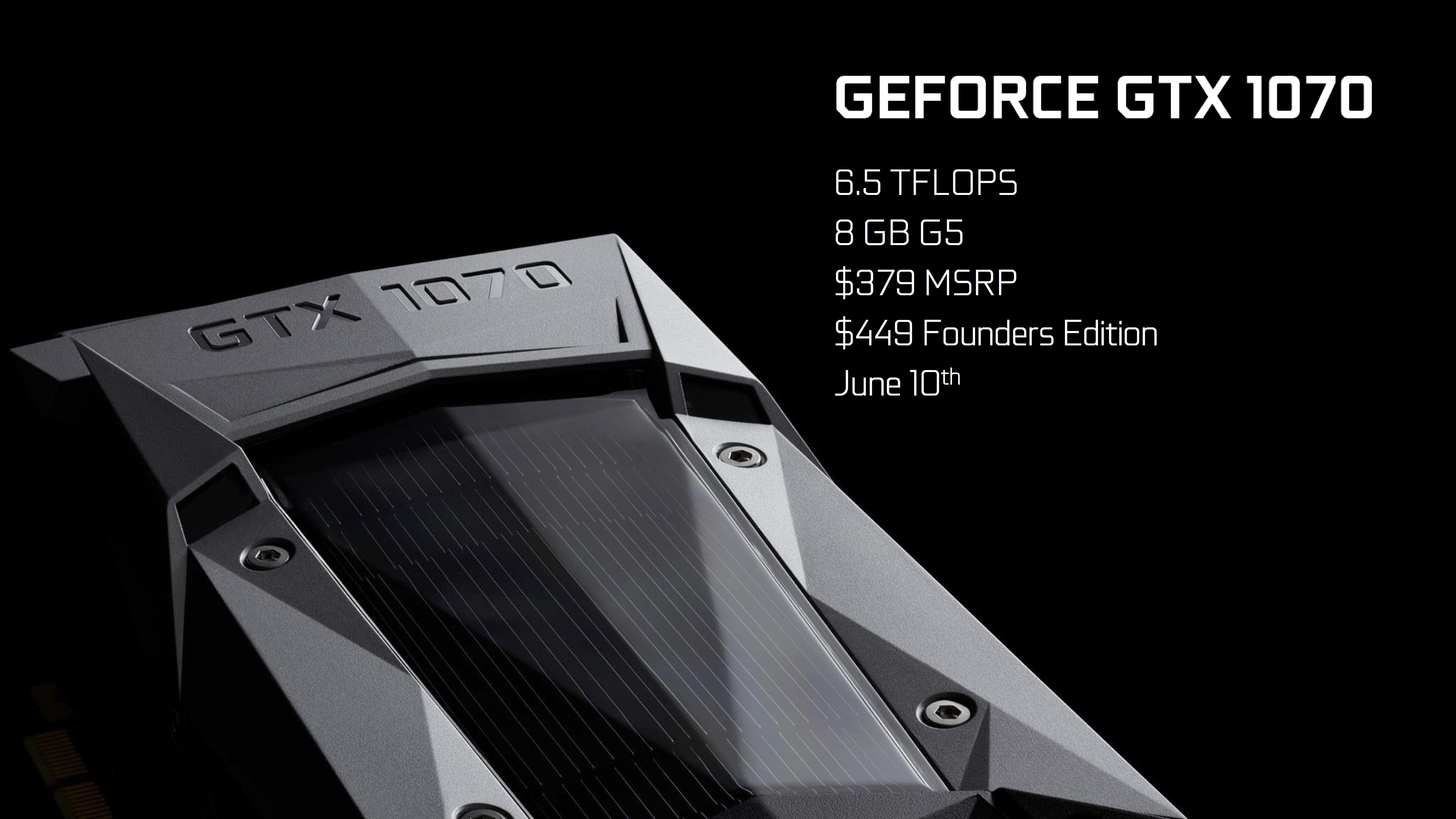
On the memory front, the card will be paired with more common GDDR5. Like the GTX 1080 there’s 8GB of VRAM, but specific clockspeeds are unknown at this time. Also unknown is the card’s TDP, though lower than GTX 1080 is a safe assumption.
Like GTX 1080, GTX 1070 will be offered in a base/MSRP version and a Founders Edition version. These will be $379 and $449 respectively – $50 over the GTX 970’s launch price of $329 – with the Founders Edition card employing the new NVIDIA industrial design. I’ll also quickly note that it remains to be seen whether the industrial design reuse will include GTX 1080’s vapor chamber, or if NVIDIA will swap out the cooling apparatus under the hood.
The GTX 1070 will be the latter of the two new Pascal cards, hitting the streets on June 10th. Like the GTX 1080, NVIDIA’s press release is very careful to only attach that date to the Founders Edition version, so we’re still waiting on confirmation over whether the base card will be available on the 10th as well.


234 Comments
View All Comments
kedesh83 - Saturday, May 7, 2016 - link
Edit: I meant that the 780 had 384bit memory bus, the graph above says 256.anubis44 - Saturday, May 7, 2016 - link
https://youtube.com/watch?v=aSYBO1BrB1INVIDIA has already lost the gaming wars. This is all pointless.
D. Lister - Sunday, May 8, 2016 - link
I believe you, but only because your reference material appears extremely credible. To hell with Nvidia, they are all but dead to me now.varad - Sunday, May 8, 2016 - link
While this video raises some valid points [having all consoles in the bag does give AMD good leverage with developers], there are some points that are inconsistent or highlight a lack of deeper understanding:The whole argument seems to be built around the "scalability" term mentioned in some AMD slide. Whoever made the video claims this means multiple smaller GPUs on a single die [connected through an interposer]. And this apparently means the volume manufacturing economics will work for AMD while NV will be stuck making larger chips with lower yields. A few thoughts and doubts on this supposed masterplan:
1. I am going to guess manufacturing with interposer based technology isn't exactly easy or cheap. This is considering that similar technology is used for HBM based GPUs today and those are mostly limited to higher end [$$$] GPUs.
2. Whoever made the video assumes that AMD would manufacture smaller GPU dies which are then connected using an interposer on a bigger die to make a high performance GPU. While this is surely possible, it also would be wasteful since there are probably multiple video [encoders/decoders] and IO [PCIE, display etc] components that do not necessarily need to be there multiple times. So this would probably require such components to then be put on a separate die. This requires more investment since such a die would then need to be manufactured and tested separately before being integrated with the regular smaller GPU dies.
3. As far as i understand, consoles have their CPU and graphics integrated on the same die. I do not think this will change because consoles are not known for high margins. So for the proposed masterplan to work, console makers either need to agree to use separate CPU & the multi-GPU dies OR AMD is able to put everything on a big die using an interposer. The former probably would not be a good idea for AMD since that would open the door for Intel + NV to capture the CPU/GPU socket. So that means the only scenario this would work for AMD is if they can connect the CPU, multiple GPUs and as explained in #2, another die for the non-replicated components using an interposer. Again, while this is technically possible, I'm not sure if it will be economically feasible.
Gigaplex - Sunday, May 8, 2016 - link
Is that why NVIDIA holds the majority of the discrete GPU market share and AMD is struggling to avoid bankruptcy?The_Assimilator - Sunday, May 8, 2016 - link
Yeah, I'm sure you and some random Youtuber are the only ones who have deduced AMD's "master plan". Certainly nVIDIA has no idea what AMD is attempting to do. /sbill44 - Saturday, May 7, 2016 - link
Is this a 10 bit card? Does it support HDR? What about audio sampling rates, hardware decode for the latest audio & video codecs (10 bit HDR h265), WCG support, HDCP 2.2, HDMI 2.0b?mdriftmeyer - Saturday, May 7, 2016 - link
Zero mention on Nvidia's site for 10-bit, or HDR, not to mention H.265 Decode/Encode.
Sorry, but Polaris curb stomps Pascal.
HDMI 2.0b, DL-DVI, HDCP 2.2 listed.
1 - 7680x4320 at 60 Hz RGB 8-bit with dual DisplayPort connectors or 7680x4320 at 60 Hz
YUV420 8-bit with on DisplayPort 1.3 connector.
2 - DisplayPort 1.2 Certified, DisplayPort 1.3/1.4 Ready.
nevcairiel - Sunday, May 8, 2016 - link
10-bit output has been supported on practically all recent NVIDIA cards, not sure what you are on about. For H265 support, they don't generally list that in the specs, but its extremely likely that it inherits the latest capabilities from the previous generation (ie. what the GTX960 offers), which would include H265 8/10-bit decode, and 8-bit encode.HDMI2.0b includes HDR support (its only metadata to inform the display of it), its up to the applications to make use of it.
wintermute000 - Sunday, May 8, 2016 - link
"but its extremely likely"For my money I'd want to be completely sure LOL