VIA's KT133A - Overclocking w/ the 133MHz FSB: The "Issue"
by Mike Andrawes on March 20, 2001 2:09 AM EST- Posted in
- Guides
The Art of Deception
But what happens if you don’t happen to own any of the aforementioned boards? Don’t give up yet; there are still ways to get around the problem. The last resort, of course, is to physically changethe default multiplier, right on your CPU. This is what was required to raise the multiplier when Socket-A overclocking first hit the streets, before the multiplier pins of the Socket-A interface were discovered. The only difference now is that we’re trying to lower the multiplier. Unfortunately, modifying the multiplier of an AMD chip is not exactly the easiest thing to do, but with the help of something we discovered by accident in the early days of Socket-A overclocking, it isn’t quite so bad.
Before jumping into the solution, we have to first revisit the bridges on a Socket-A CPU and see how multiplier ratios are actually set. On any Socket-A chip, you will find three sets of bridges that control the default multiplier relayed to the motherboard: L3, L4, and L6. The L6 bridge refers to the Frequency ID pins (FID) and the L3 and L4 Bridges refer to the BP_FID pins. Basically by manipulating these three sets of bridges, you can change the clock multiplier of the CPU all the way from 5 to 12.5 (in 0.5 increments).
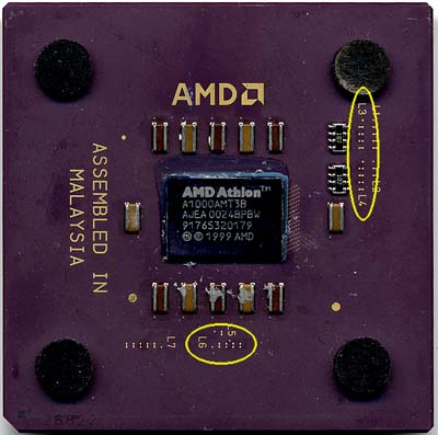
The locations of L3, L4, and L6 bridges on a Socket-A CPU
So theoretically in order to make your chip having a lower multiplier, you just need to follow the Frequency Selection chart in the article from Tom’s Hardware. However, when modifying those bridges, oftentimes the hardest thing to do is to cut one of these bridges. Connecting an already broken bridge is simple enough, since it can be done with a mechanical pencil or a conductive pen. Cutting a bridge can actually be dangerous, as the tools required to do so could actually damage the CPU.
Therefore, the ideal solution would minimize the number of bridges that need to be cut, while at the same time achieving our goal of lowering the default clock multiplier. Back in our AMD Thunderbird / Duron Investigation and Overclocking Discussion, we accidentally thought that the jumpers on the FIC AD-11 were in charge of the FID pins, when in fact they controlled the BP_FID pins. The result of that is we weren’t able to raise the multiplier any higher than the default, even though we could lower the multiplier.
That piece of information gave us a big hint - even if the FID pins and the
BP_FID pins do not match, the chip will still work. So it is possible for us
to modify either set of bridges to lower the multiplier. Since the L6 bridge
controls the default clock multiplier and it has only four pairs, it is the
best candidate for us to play with. Keep in mind that our goal is to let the
chip boot up at a lower multiplier for a few clock cycles so that the settings
from the BIOS come in and take charge.


0 Comments
View All Comments