VIA Apollo Pro 133: A Camino Preview
by Anand Lal Shimpi on August 16, 1999 6:03 AM EST- Posted in
- Motherboards
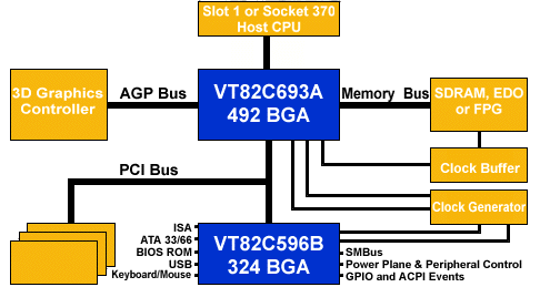
North/South Bridge vs Accelerated Hub Architecture
Since the dawn of the single chip solution, the idea of creating chipset solutions with interchangeable "parts" was the goal in order to keep flexibility at a maximum. The theory was then translated into what is now known as the North/South bridge architecture, where the main memory/graphics controller is housed in a chip that makes up the North bridge and all I/O functions are handled in a chip known as the South bridge. In theory, a single North bridge could be coupled with one of three different south bridges in order to tailor to the needs of various types of computer users. In practice, no chipset manufacturer has truly used this technology to its full potential.
VIA has started to do so with their two most popular south bridges, the Mobile South Bridge (VT82C596A) or the Super South Bridge (VT82C686A) controller. The main difference between the two south bridges is that the Super South Bridge offers support for AMR (Audio Modem Riser - see Intel 810 Review) as well as Ultra ATA 66, a feature currently only supported in one of Intel's chipsets, the 810 and due for support in the 820 (Camino). The beauty behind this design is that it doesn't cost motherboard manufacturers very much to implement the Super South Bridge in their designs that already feature the Mobile South Bridge. As soon as VIA ramps up production on the Super South Bridge parts, the motherboard manufacturers can then use the new south bridge in their designs and sell all of their boards that feature the older south bridge at a lower cost while offering the boards equipped with the newer south bridge at an increased cost.
But why stop there? In theory (don't you love those two words?), if the demand were high enough, VIA's Firewire controller could be integrated into the south bridge design and motherboard manufacturers would then have the option of selling a third type of Apollo Pro 133 based motherboard with integrated Firewire. Or, if the demand for on-board Ethernet were great enough, VIA could integrate Ethernet functionality into the south bridge thus increasing the number of options users would have when going after a motherboard based on a VIA chipset. The possibilities are endless, and moving the chipset design to a 0.18 micron fabrication process just increases the amount of room VIA will have to work with. But why doesn't VIA just go ahead and do it? As alluded to above, the demand just isn't there, for a manufacturer to make such a move they would have to weigh out the costs of implementation vs the resulting increase in sales, and currently, the numbers just aren't working. VIA is definitely aware of the potential, as quite a few of their representatives were preaching to the crowd about the possibilities at last year's Fall Comdex, it's just a matter of time before it happens.


0 Comments
View All Comments