The Intel Xeon E7-8800 v3 Review: The POWER8 Killer?
by Johan De Gelas on May 8, 2015 8:00 AM EST- Posted in
- CPUs
- IT Computing
- Intel
- Xeon
- Haswell
- Enterprise
- server
- Enterprise CPUs
- POWER
- POWER8
Haswell Architecture Improvements
We have discussed the advantages that the Haswell core brings here in more detail. In a nutshell:
- The core can sustain about 10% more integer instructions per clock cycle than its predecessor, Ivy Bridge.
- Virtualized applications should perform slightly better thanks to the lower VM exit/entry latency.
- HPC applications could/should benefit much more if they are recompiled to make use of the improved AVX2 and Fused Multiply Add (FMA) support
- Database transactional applications should benefit more thanks to the lower synchronization latency.
- In-memory databases should benefit if they are adapted to make use of the AVX-2 256 bit integer vector operations.
Again, the same is true about the Xeon E5-2600v3. So what makes the E7 special?
Transactional Synchronization Extensions: I'll be back
There is one "new" - or rather "now working" - feature: TSX or the famous Transactional Synchronization eXtensions. These extensions are all about making locking more "optimistic" (you let the CPU handle the bookkeeping to maintain consistency). TSX is quite powerful, but also can be a liability in the wrong use case. Developers will need a deep understanding of the locking and parallel programming to be able to make good use of TSX, as
- ... you still have to rewrite your code (inserting hints)
- TSX may reduce performance in some situations: if indeed a pessimistic lock was necessary, the transaction has to be re-executed with a "traditional" conservative way of locking. You could call it a "lock misprediction".
Introducing TSX in software requires assessing the different locks in application, using different libraries and quite a bit of of tuning. SAP and Intel did this for the expensive in-memory data mining SAP HANA software.
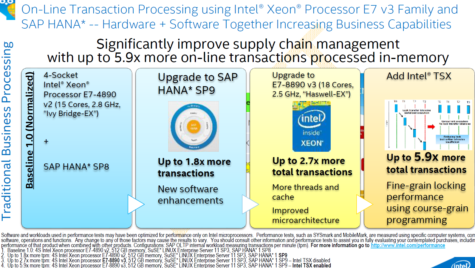
The upgrade from "Ivy Bridge EX" to "Haswell-EX" yielded 50% performance, while introducing TSX roughly doubled performance. So in TSX enabled data mining software, Haswell-EX has the potential to reduce the waiting time by a factor of 3 and more.


146 Comments
View All Comments
PowerTrumps - Saturday, May 9, 2015 - link
I'm sure the author will update the article unless this was a Intel cheerleading piece.name99 - Friday, May 8, 2015 - link
The thing is called E7-8890. Not E7-5890?WTF Intel? Is your marketing team populated by utter idiots? Exactly what value is there in not following the same damn numbering scheme that your product line has followed for the past eight years or so?
Something like that makes the chip look like there's a whole lot of "but this one goes up to 11" thinking going on at Intel...
name99 - Friday, May 8, 2015 - link
OK, I get it. The first number indicates the number of glueless chips, not the micro-architecture generation. Instead we do that (apparently) with a v2 or v3 suffix.I still claim this is totally idiotic. Far more sensible would be to use the same scheme as the other Intel processors, and use a suffix like S2, S4, S8 to show the glueless SMP capabilities.
ZeDestructor - Friday, May 8, 2015 - link
They've been using this convention since Westmere-EX actually, at which point they ditched their old convention of a prefix letter for power tier, followed by one digit for performance/scalability tier, followed by another digit for generation then the rest for individual models. Now we have 2xxx for dual socket, 4xxx for quad socket and 8xxx for 8+ sockets, and E3/E5/E7 for the scalability tier. I'm fine with either, though I have a slight preference for the current naming scheme because the generation is no longer mixed into the main model number.Morawka - Saturday, May 9, 2015 - link
man the power 8 is a beefy cpu... all that cache, you'd think it would walk all over intel.. but intel's superior cpu design winsPowerTrumps - Saturday, May 9, 2015 - link
please explaintsk2k - Saturday, May 9, 2015 - link
Where are the gaming benchmarks?JohanAnandtech - Saturday, May 9, 2015 - link
Is there still a game with software rendering? :-)Gigaplex - Sunday, May 10, 2015 - link
Llvmpipe on Linux gives a capable (feature wise) OpenGL implementation on the CPU.Klimax - Saturday, May 9, 2015 - link
Don't see POWER getting anywhere with that kind of TDP. There will be dearth of datacenters and other hosting locations retooling for such thing. And I suspect not many will even then take it as cooling and power costs will be damn too high.Problem is, IBM can't go lower with TDP as architecture features enabling such performance are directly responsible for such TDP. (Just L1 consumes 2W to keep few cycles latency at high frequency)