The Samsung Galaxy S6 and S6 edge Review
by Joshua Ho on April 17, 2015 9:00 AM EST- Posted in
- Smartphones
- Samsung
- Mobile
- Galaxy S6
- Galaxy S6 Edge
Exynos 7420: First 14nm Silicon In A Smartphone
This generation more than any generation in recent memory has been a time of significant movement in the SoC space. We were aware of the Exynos 7420 well before it was announced in the Galaxy S6, but for the most part I expected to see Snapdragon 810 in at least a few variants of the Galaxy S6. It was a bit surprising to see Samsung drop Snapdragon SoCs completely this generation, and judging by the battery life of the Galaxy S6 it seems that Samsung had their reasons for doing this.
For those that are unfamiliar with the Exynos 7420, this SoC effectively represents the culmination of their efforts in semiconductor manufacturing and integrated circuit design. On the foundry side, Samsung is leveraging their vertical integration to make the first SoC on their 14nm LPE (Low Power Early) process, which seems to be solely for Systems LSI until they can no longer use all production capacity.
We previously mentioned that Samsung’s 14nm process in general will lack any significant die shrink due to almost unchanged metal interconnect pitch, but this assumption was in comparison to their 20nm LPM process from which the 14nm LPE process borrows its BEOL (back end of line) from. Opposite to what we thought, the Exynos 5433 was manufacturered on a 20LPE process which makes use of a quite larger metal layer. The result is that one can see a significant die shrink for the 7420 as it is, according to Chipworks, only 78mm² and a 44% reduction over the Exynos 5433's 113mm². This is considerable even when factoring in that the new SoC had two added GPU shader cores. Beyond the swap from a LPDDR3 memory controller to a LPDDR4 capable one, the only other at first noticeable major functional overhaul on the SoC seems to be that the dedicated HEVC decoder block has been removed and HEVC encoding and decoding capability has been merged into Samsung's MFC (Multi-Function Codec) media hardware acceleration block.
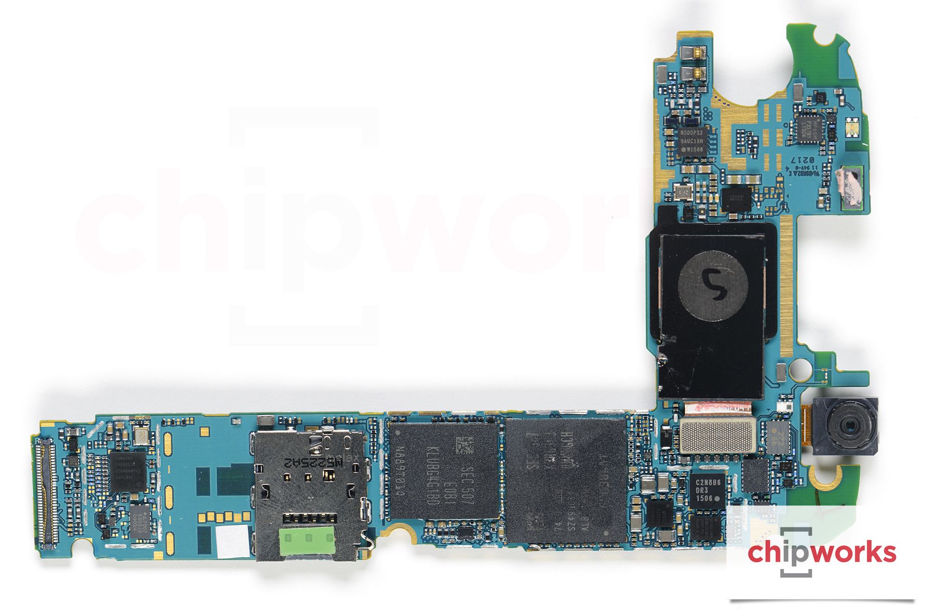
Galaxy S6 PCB with SoC and modem in view (Source: Chipworks)
The move from a planar to FinFET process is crucial. Although this is covered in more detail in previous articles, the short explanation is that planar processes suffer from increasing power leakage at smaller process nodes as the bulk of the silicon becomes relatively more massive than the gate that controls the flow of current. This causes decreased power efficiency as the power source of the transistor starts to act as a gate itself. FinFET solves this problem by attempting to isolate the transistor from the bulk of the silicon wafer, wrapping the gate around the channel of the transistor to ensure that it retains strong control over the flow of current compared to a planar transistor design.
The effective voltage drop allowed by the process can be substantial. We can have a look at some voltage excerpts of common frequencies available on both the Exynos 5433 and 7420:
| Exynos 5433 vs Exynos 7420 Supply Voltages | ||||||
| Exynos 5433 | Exynos 7420 | Difference | ||||
| A57 1.9GHz (ASV2) | 1287.50mV | 1056.25mV | -234.25mV | |||
| A57 1.9GHz (ASV9) | 1200.00mV | 975.00mV | -225.00mV | |||
| A57 1.9GHz (ASV15) | 1125.00mV | 912.50mV | -212.50mV | |||
| A57 800MHz (ASV2) | 950.00mV | 768.75mV | -181.25mV | |||
| A57 800MHz (ASV9) | 900.00mV | 687.50mV | -224.50mV | |||
| A57 800MHz (ASV15) | 900.00mV | 625.00mV | -275.00mV | |||
| A53 1.3GHz (ASV2) | 1200.00mV | 1037.50mV | -162.50mV | |||
| A53 1.3GHz (ASV9) | 1112.50mV | 950.00mV | -162.50mV | |||
| A53 1.3GHz (ASV15) | 1062.50mV | 900.00mV | -162.50mV | |||
| A53 400MHz (ASV2) | 862.00mV | 743.75mV | -118.25mV | |||
| A53 400MHz (ASV9) | 787.50mV | 656.25mV | -131.25mV | |||
| A53 400MHz (ASV15) | 750.00mV | 606.25mV | -143.75mV | |||
| GPU 700MHz (ASV2) | 1125.00mV | 881.25mV | -243.75mV | |||
| GPU 700MHz (ASV9) | 1050.00mV | 800.00mV | -250.00mV | |||
| GPU 700MHz (ASV15) | 1012.50mV | 750.00mV | -262.50mV | |||
| GPU 266MHz (ASV2) | 875.00mV | 750.00mV | -125.00mV | |||
| GPU 266MHz (ASV9) | 800.00mV | 668.75mV | -131.25mV | |||
| GPU 266MHz (ASV15) | 762.50mV | 606.25mV | -156.25mV | |||
The ASV (Adaptive Scaling Voltage) numbers represent the different type of chip bins, a lower value representing a worse quality bin and a higher one a better quality one. Group 2 should be the lowest that is found in the wild, with group 15 representing the best possible bin and group 9 the median that should be found in most devices. As one can see in the table, we can achieve well up to -250mV voltage drop on some frequencies on the A57s and the GPU. As a reminder, power scales quadratically with voltage, so a drop from 1287.50mV to 1056.25mV as seen in the worst bin 1.9GHz A57 frequency should for example result in a considerable 33% drop in dynamic power. The Exynos 7420 uses this headroom to go slightly higher in clocks compared to the 5433 - but we expect the end power to still be quite lower than what we've seen on the Note 4.
On the design side, Systems LSI has also done a great deal to differentiate the Exynos 7420 from the 5433. Although the CPU architectures are shared, the A53 cluster is now clocked at 1.5 GHz instead of 1.3 GHz, and the A57 cluster at 2.1 GHz rather than 1.9 GHz. The memory controller is new and supports LPDDR4 running at 1555MHz. This means that the Galaxy S6 has almost double the theoretical memory bandwidth when compared to the Galaxy Note 4 Exynos variant, as we get a boost up to 24.88GB/s over the 5433's 13.20GB/s. We still need to test this to see how these claims translate to practical performance in a deep dive article in the future, as effective bandwidth and latency can often vary depending on vendor's memory settings and SoC's bus architecture.
Outside of the memory controller, LSI has also updated the 7420 to use a more powerful Mali T760MP8 GPU. Although the Exynos 5433 had a Mali T760 GPU as well, it had two fewer shader cores which means that achieving a given level of performance requires higher clock speeds and higher voltages to overcome circuit delay. This new GPU is clocked a bit higher as well, at 772 MHz compared to the 700 MHz of the GPU in the Exynos 5433. We see the same two-stage maximum frequency scaling mechanism as discovered in our Note 4 Exynos review, with less ALU biased loads being limited to 700MHz as opposed to the 5433's 600MHz. There's also a suspicion that Samsung was ready to go higher to compete with other vendors though, as we can see evidence of an 852 MHz clock state that is unused. Unfortunately deeply testing this SoC isn’t possible at this time as doing so would require disassembling the phone.


306 Comments
View All Comments
akdj - Friday, April 24, 2015 - link
That's NOT the same display. The Note 4 was a step up from 5Active and this is an even bigger step 'up' for AMOLED. The anomalies have been talked about in many reviews. As well as some purple fringing shooting low light (w/light source, like a candle). Killer display though!Refuge - Friday, April 17, 2015 - link
I'm not entirely sure, I kind wish he had elaborated more on it. Especially when this is a flagship phone and he says there is a defect with the perfect screen.But they only thing I can think of is how it seems to reflect much like a bubble would in direct sunlight. Maybe there is a risk of this rainbow effect screwing with color accuracy in direct sunlight? I'm not entirely sure either.
Ammaross - Friday, April 17, 2015 - link
I see two vertical dark bars on left and right sides of the screen and one 1/4 from the top horizontally. Maybe that's what he's referring to...Peichen - Saturday, April 18, 2015 - link
I see the same thing as Ammaross. I guess some of you need to have your screen calibrated. I can see the dark bars on my home PC but I guess I won't be able to see it on the cheap/crap workstation at work.Maxpower2727 - Friday, April 17, 2015 - link
The only thing I saw in that photo was reflected light, which is to be expected with any phone and could hardly be considered a "defect." I really don't understand what he was getting at with that.JoshHo - Friday, April 17, 2015 - link
It was surprisingly hard to capture, but it's the photo of the horizontal/vertical bars when the display was under strong sunlight.arayoflight - Friday, April 17, 2015 - link
Josh, I think the front facing camera has a1/4.1" sensor, not 1/3". It was conformed by Samsung tomorrow.Also, the IMX240 has 1.2 micron pixels, not 1.12.
Correct these 2 mistakes. The review was great though.
JoshHo - Friday, April 17, 2015 - link
Apologies. I have fixed the FFC sensor size.To my knowledge the IMX240 uses 1.12 micron pixel size, going by Chipworks measurements and the released spec for the S5K2P2 sensor which has the same pixel count and sensor size.
arayoflight - Saturday, April 18, 2015 - link
The s5k2p2 has 1.12 micron size. Also they're both 1/2.6" and identical resolution.But 1/2.6" necessarily doesn't mean they're same size. It just tells the size of the disk and hence there can be a difference.
I think also on the Wiki page of IMX240 it's 1.2 micron. Though it's a different 4:3 IMX240 but I doubt they'll change the pixel pitch for a custom IMX240 used by Samsung.
Just look into it. Even I want to know the perfect pixel size :)
will54 - Monday, April 20, 2015 - link
Its the one horizontal stripe and the 2 vertical stripes on each side of the screen