The NVIDIA GeForce GTX 980 Review: Maxwell Mark 2
by Ryan Smith on September 18, 2014 10:30 PM ESTMaxwell 1 Architecture: The Story So Far
Before we dive into the story and architecture of Maxwell 2, we’d like to spend a bit of time recapping what we’ve seen so far with Maxwell 1 and the GM107 GPU. While both GPUs are distinctly Maxwell, Maxwell 2 is essentially a second, more feature-packed version of Maxwell. Meanwhile it retains all of the base optimizations that went into Maxwell 1, implemented on a larger scale for a larger GPU.
Beginning with the Maxwell family of architectures, NVIDIA embarked on a “mobile first” design strategy for GPUs, marking a significant change in NVIDIA’s product design philosophy. As of Maxwell NVIDIA’s top-down philosophy that saw the launch of high-end desktop class GPUs come first has come to an end, and as NVIDIA has chosen to embrace power efficiency and mobile-friendly designs as the foundation of their GPU architectures, this has led to them going mobile first on Maxwell. With Maxwell NVIDIA has made the complete transition from top to bottom, and are now designing GPUs bottom-up instead of top-down.
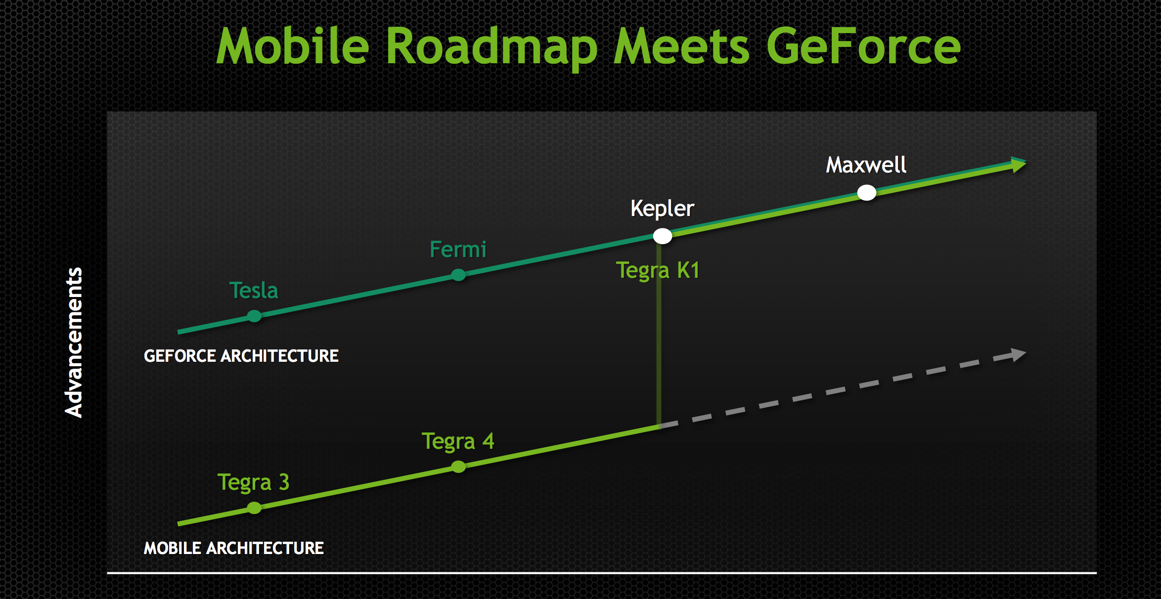
By going mobile first NVIDIA is aiming to address several design considerations at all once. First and foremost is the fact that NVIDIA is heavily staking the future of their company in mobile, and that means they need GPU designs suitable for such a market. This mobile first view is primarily focused on SoC-class products – the Tegra family – but really it even extends to mobile PC form factors such as laptops, where discrete GPUs can play an important role but are going to have strict thermal requirements. By designing GPUs around mobile first, NVIDIA starts with a design that is already suitable for Tegra and then can scale it up as necessary for laptop and desktop GeForce products. Graphics is – as we like to say – embarrassingly parallel, so if you can build one small module then it’s relatively easy to scale up performance by building chips with more modules and tying them together. This is the mobile first philosophy.
What this means is that NVIDIA is focused on power efficiency more than ever before. The SoC market is brutal for both the demands placed on the hardware and for the competitive nature of that market, and given the fact that SoCs are so heavily constrained by thermal and power considerations, every bit of power saved can be reinvested in additional performance. This in turn calls for a GPU that is especially power efficient, as it is efficiency that will win the market for NVIDIA.
Maxwell then is an interesting take on NVIDIA’s designs that does not radically alter NVIDIA’s architecture, but has had every accommodation made to improve energy efficiency. The result is a Kepler-like architecture with a number of small design tweaks that improve efficiency in some manner. As NVIDIA tells it, there is no single aspect of Maxwell that is disproportionally responsible for NVIDIA’s energy improvements, but rather it is the culmination of these small changes. Through these changes NVIDIA has been able to come close to doubling their performance per watt versus Kepler, which is nothing short of amazing given the fact that all of this is being done on the same 28nm process as Kepler.
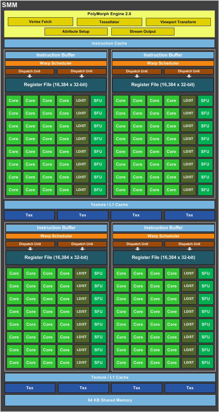
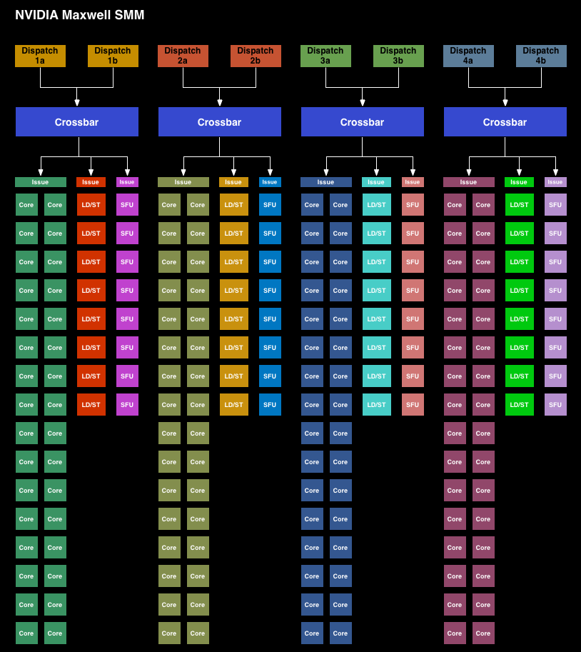
Starting with the Maxwell 1 SMM, NVIDIA has adjusted their streaming multiprocessor layout to achieve better efficiency. Whereas the Kepler SMX was for all practical purposes a large, flat design with 4 warp schedulers and 15 different execution blocks, the SMM has been heavily partitioned. Physically each SMM is still one contiguous unit, not really all that different from an SMX. But logically the execution blocks which each warp scheduler can access have been greatly curtailed.
The end result is that in an SMX the 4 warp schedulers would share most of their execution resources and work out which warp was on which execution resource for any given cycle. But on an SMM, the warp schedulers are removed from each other and given complete dominion over a far smaller collection of execution resources. No longer do warp schedulers have to share FP32 CUDA cores, special function units, or load/store units, as each of those is replicated across each partition. Only texture units and FP64 CUDA cores are shared.
Among the changes NVIDIA made to reduce power consumption, this is among the greatest. Shared resources, though extremely useful when you have the workloads to fill them, do have drawbacks. They’re wasting space and power if not fed, the crossbar to connect all of them is not particularly cheap on a power or area basis, and there is additional scheduling overhead from having to coordinate the actions of those warp schedulers. By forgoing the shared resources NVIDIA loses out on some of the performance benefits from the design, but what they gain in power and space efficiency more than makes up for it.
NVIDIA still isn’t sharing hard numbers on SMM power efficiency, but for space efficiency a single 128 CUDA core SMM can deliver 90% of the performance of a 192 CUDA core SMX at a much smaller size.
Moving on, along with the SMM layout changes NVIDIA has also made a number of small tweaks to improve the IPC of the GPU. The scheduler has been rewritten to avoid stalls and otherwise behave more intelligently. Furthermore by achieving higher utilization of their existing hardware, NVIDIA doesn’t need as many functional units to hit their desired performance targets, which in turn saves on space and ultimately power consumption.
NVIDIA has also been focused on memory efficiency, both for performance and power reasons, resulting in the L2 cache size been greatly increased. NVIDIA has from 256KB in GK107 to 2MB on GM107, and from 512KB on GK104 to the same 2MB on GM204. This cache size increase reduces the amount of traffic that needs to cross the memory bus, reducing both the power spent on the memory bus and improving overall performance.
Increasing the amount of cache always represents an interesting tradeoff since cache is something of a known quantity and is rather dense, but it’s only useful if there are memory stalls or other memory operations that it can cover. Consequently we often see cache implemented in relation to whether there are any other optimizations available. In some cases it makes more sense to use the transistors to build more functional units, and in other cases it makes sense to build the cache. The use of 2MB of L2 cache in both GM107 and GM204 – despite the big differences in ROP count and memory bus size – indicates that NVIDIA’s settling on 2MB as their new sweet spot for consumer graphics GPUs.
Finally there’s the lowest of low level optimizations, which is transistor level optimizations. These optimizations are something of a secret sauce for NVIDIA, but they tell us they’ve gone through at the transistor level to squeeze out additional energy efficiency as they could find it. Given that TSMC 28nm is now a very mature process with well understood abilities and quirks, NVIDIA should be able to design and build their circuits to a tighter tolerance now than they would have been able to when working on GK107 and GK104 over 2 years ago.


274 Comments
View All Comments
garadante - Sunday, September 21, 2014 - link
What might be interesting is doing a comparison of video cards for a specific framerate target to (ideally, perhaps it wouldn't actually work like this?) standardize the CPU usage and thus CPU power usage across greatly differing cards. And then measure the power consumed by each card. In this way, couldn't you get a better example ofgaradante - Sunday, September 21, 2014 - link
Whoops, hit tab twice and it somehow posted my comment. Continued:couldn't you get a better example of the power efficiency for a particular card and then meaningful comparisons between different cards? I see lots of people mentioning how the 980 seems to be drawing far more watts than it's rated TDP (and I'd really like someone credible to come in and state how heat dissipated and energy consumed are related. I swear they're the exact same number as any energy consumed by transistors would, after everything, be released as heat, but many people disagree here in the comments and I'd like a final say). Nvidia can slap whatever TDP they want on it and it can be justified by some marketing mumbo jumbo. Intel uses their SDPs, Nvidia using a 165 watt TDP seems highly suspect. And please, please use a nonreference 290X in your reviews, at least for a comparison standpoint. Hasn't it been proven that having cooling that isn't garbage and runs the GPU closer to high 60s/low 70s can lower power consumption (due to leakage?) something on the order of 20+ watts with the 290X? Yes there's justification in using reference products but lets face it, the only people who buy reference 290s/290Xs were either launch buyers or people who don't know better (there's the blower argument but really, better case exhaust fans and nonreference cooling destroys that argument).
So basically I want to see real, meaningful comparisons of efficiencies for different cards at some specific framerate target to standardize CPU usage. Perhaps even monitoring CPU usage over the course of the test and reporting average, minimum, peak usage? Even using monitoring software to measure CPU power consumption in watts (as I'm fairly sure there are reasonably accurate ways of doing this already, as I know CoreTemp reports it as its probably just voltage*amperage, but correct me if I'm wrong) and reported again average, minimum, peak usage would be handy. It would be nice to see if Maxwell is really twice as energy efficient as GCN1.1 or if it's actually much closer. If it's much closer all these naysayers prophesizing AMD's doom are in for a rude awakening. I wouldn't put it past Nvidia to use marketing language to portray artificially low TDPs.
silverblue - Sunday, September 21, 2014 - link
Apparently, compute tasks push the power usage way up; stick with gaming and it shouldn't.fm123 - Friday, September 26, 2014 - link
Don't confuse TDP with power consumption, they are not the same thing. TDP is for designing the thermal solution to maintain the chip temperature. If there is more headroom in the chip temperature, then the system can operate faster, consuming more power."Intel defines TDP as follows: The upper point of the thermal profile consists of the Thermal Design Power (TDP) and the associated Tcase value. Thermal Design Power (TDP) should be used for processor thermal solution design targets. TDP is not the maximum power that the processor can dissipate. TDP is measured at maximum TCASE"
https://www.google.com/url?sa=t&source=web&...
NeatOman - Sunday, September 21, 2014 - link
I just realized that the GTX 980 has a TDP of 165 watts, my Corsair CX430 watt PSU is almost overkill!, that's nuts. That's even enough room to give the whole system a very good stable overclock. Right now i have a pair of HD 7850's @ stock speed and a FX-8320 @ 4.5Ghz, good thing the Corsair puts out over 430 watts perfectly clean :)Nfarce - Sunday, September 21, 2014 - link
While a good power supply, you are leaving yourself little headroom with 430W. I'm surprised you are getting away with it with two 7850s and not experiencing system crashes.ET - Sunday, September 21, 2014 - link
The 980 is an impressive feat of engineering. Fewer transistors, fewer compute units, less power and better performance... NVIDIA has done a good job here. I hope that AMD has some good improvements of its own under its sleeve.garadante - Sunday, September 21, 2014 - link
One thing to remember is they probably save a -ton- of die area/transistors by giving it only what, 1/32 double precision rate? I wonder how competitive in terms of transistors/area an AMD GPU would be if they gutted double precision compute and went for a narrower, faster memory controller.Farwalker2u - Sunday, September 21, 2014 - link
I am looking forward to your review of the GTX 970 once you have a compatible sample in hand.I would like to see the results of the Folding @Home benchmarks. It seems that this site is the only one that consistently use that benchmark in its reviews.
As a "Folder" I'd like to see any indication that the GTX 970, at a cost of $330 and drawing less watts than a GTX 780; may out produce both the 780 ($420 - $470) and the 780Ti ($600). I will be studying the Folding @ Home: Explicit, Single Precision chart which contains the test results of the GTX 970.
Wolfpup - Monday, September 22, 2014 - link
Wow, this is impressive stuff. 10% more performance from 2/3 the power? That'll be great for desktops, but of course even better for notebooks. Very impressed they could pulll off that kind of leap on the same process!They've already managed to significantly bump up the top end mobile part from GTX 680 -> 880, but within a year or so I bet they can go quite a bit higher still.
Oh well, it was nice having a top of the line mobile GPU for a while LOL
If 28nm hit in 2012 though, doesn't that make 2015 its third year? At least 28nm seems to be a really good process, vs all the issues with 90/65nm, etc., since we're stuck on it so long.
Isn't this Moore's Law hitting the constraints of physical reality though? We're taking longer and longer to get to progressively smaller shrinks in die size, it seems like...
Oh well, 22nm's been great with Intel and 28's been great with everyone else!