The NVIDIA GeForce GTX 980 Review: Maxwell Mark 2
by Ryan Smith on September 18, 2014 10:30 PM ESTMaxwell 1 Architecture: The Story So Far
Before we dive into the story and architecture of Maxwell 2, we’d like to spend a bit of time recapping what we’ve seen so far with Maxwell 1 and the GM107 GPU. While both GPUs are distinctly Maxwell, Maxwell 2 is essentially a second, more feature-packed version of Maxwell. Meanwhile it retains all of the base optimizations that went into Maxwell 1, implemented on a larger scale for a larger GPU.
Beginning with the Maxwell family of architectures, NVIDIA embarked on a “mobile first” design strategy for GPUs, marking a significant change in NVIDIA’s product design philosophy. As of Maxwell NVIDIA’s top-down philosophy that saw the launch of high-end desktop class GPUs come first has come to an end, and as NVIDIA has chosen to embrace power efficiency and mobile-friendly designs as the foundation of their GPU architectures, this has led to them going mobile first on Maxwell. With Maxwell NVIDIA has made the complete transition from top to bottom, and are now designing GPUs bottom-up instead of top-down.
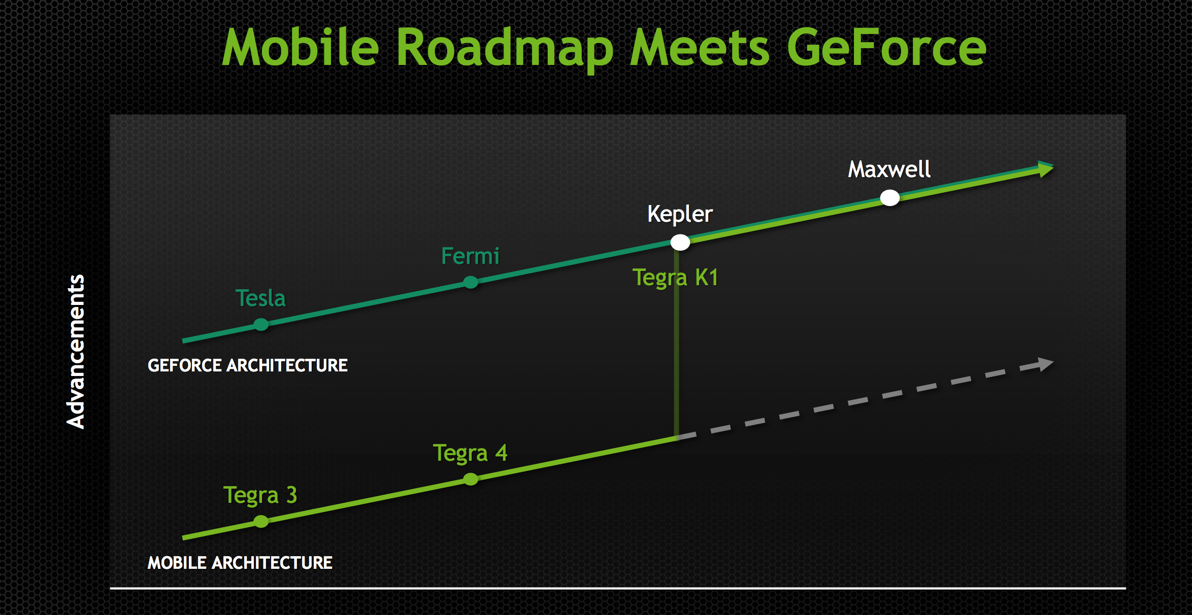
By going mobile first NVIDIA is aiming to address several design considerations at all once. First and foremost is the fact that NVIDIA is heavily staking the future of their company in mobile, and that means they need GPU designs suitable for such a market. This mobile first view is primarily focused on SoC-class products – the Tegra family – but really it even extends to mobile PC form factors such as laptops, where discrete GPUs can play an important role but are going to have strict thermal requirements. By designing GPUs around mobile first, NVIDIA starts with a design that is already suitable for Tegra and then can scale it up as necessary for laptop and desktop GeForce products. Graphics is – as we like to say – embarrassingly parallel, so if you can build one small module then it’s relatively easy to scale up performance by building chips with more modules and tying them together. This is the mobile first philosophy.
What this means is that NVIDIA is focused on power efficiency more than ever before. The SoC market is brutal for both the demands placed on the hardware and for the competitive nature of that market, and given the fact that SoCs are so heavily constrained by thermal and power considerations, every bit of power saved can be reinvested in additional performance. This in turn calls for a GPU that is especially power efficient, as it is efficiency that will win the market for NVIDIA.
Maxwell then is an interesting take on NVIDIA’s designs that does not radically alter NVIDIA’s architecture, but has had every accommodation made to improve energy efficiency. The result is a Kepler-like architecture with a number of small design tweaks that improve efficiency in some manner. As NVIDIA tells it, there is no single aspect of Maxwell that is disproportionally responsible for NVIDIA’s energy improvements, but rather it is the culmination of these small changes. Through these changes NVIDIA has been able to come close to doubling their performance per watt versus Kepler, which is nothing short of amazing given the fact that all of this is being done on the same 28nm process as Kepler.
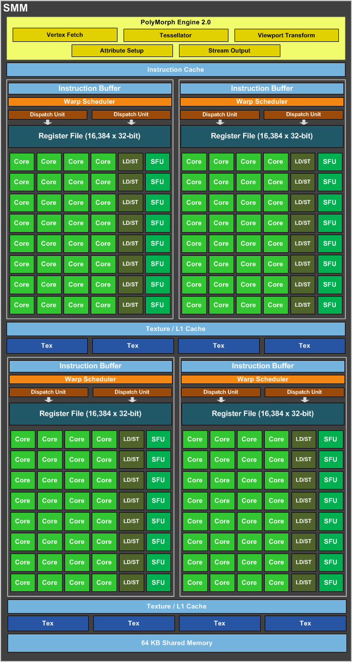
Starting with the Maxwell 1 SMM, NVIDIA has adjusted their streaming multiprocessor layout to achieve better efficiency. Whereas the Kepler SMX was for all practical purposes a large, flat design with 4 warp schedulers and 15 different execution blocks, the SMM has been heavily partitioned. Physically each SMM is still one contiguous unit, not really all that different from an SMX. But logically the execution blocks which each warp scheduler can access have been greatly curtailed.
The end result is that in an SMX the 4 warp schedulers would share most of their execution resources and work out which warp was on which execution resource for any given cycle. But on an SMM, the warp schedulers are removed from each other and given complete dominion over a far smaller collection of execution resources. No longer do warp schedulers have to share FP32 CUDA cores, special function units, or load/store units, as each of those is replicated across each partition. Only texture units and FP64 CUDA cores are shared.
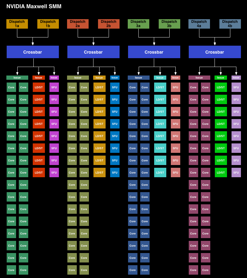
Among the changes NVIDIA made to reduce power consumption, this is among the greatest. Shared resources, though extremely useful when you have the workloads to fill them, do have drawbacks. They’re wasting space and power if not fed, the crossbar to connect all of them is not particularly cheap on a power or area basis, and there is additional scheduling overhead from having to coordinate the actions of those warp schedulers. By forgoing the shared resources NVIDIA loses out on some of the performance benefits from the design, but what they gain in power and space efficiency more than makes up for it.
NVIDIA still isn’t sharing hard numbers on SMM power efficiency, but for space efficiency a single 128 CUDA core SMM can deliver 90% of the performance of a 192 CUDA core SMX at a much smaller size.
Moving on, along with the SMM layout changes NVIDIA has also made a number of small tweaks to improve the IPC of the GPU. The scheduler has been rewritten to avoid stalls and otherwise behave more intelligently. Furthermore by achieving higher utilization of their existing hardware, NVIDIA doesn’t need as many functional units to hit their desired performance targets, which in turn saves on space and ultimately power consumption.
NVIDIA has also been focused on memory efficiency, both for performance and power reasons, resulting in the L2 cache size been greatly increased. NVIDIA has from 256KB in GK107 to 2MB on GM107, and from 512KB on GK104 to the same 2MB on GM204. This cache size increase reduces the amount of traffic that needs to cross the memory bus, reducing both the power spent on the memory bus and improving overall performance.
Increasing the amount of cache always represents an interesting tradeoff since cache is something of a known quantity and is rather dense, but it’s only useful if there are memory stalls or other memory operations that it can cover. Consequently we often see cache implemented in relation to whether there are any other optimizations available. In some cases it makes more sense to use the transistors to build more functional units, and in other cases it makes sense to build the cache. The use of 2MB of L2 cache in both GM107 and GM204 – despite the big differences in ROP count and memory bus size – indicates that NVIDIA’s settling on 2MB as their new sweet spot for consumer graphics GPUs.
Finally there’s the lowest of low level optimizations, which is transistor level optimizations. These optimizations are something of a secret sauce for NVIDIA, but they tell us they’ve gone through at the transistor level to squeeze out additional energy efficiency as they could find it. Given that TSMC 28nm is now a very mature process with well understood abilities and quirks, NVIDIA should be able to design and build their circuits to a tighter tolerance now than they would have been able to when working on GK107 and GK104 over 2 years ago.


274 Comments
View All Comments
TheJian - Saturday, September 20, 2014 - link
http://blogs.nvidia.com/blog/2014/09/19/maxwell-an...Did I miss it in the article or did you guys just purposely forget to mention NV claims it does DX12 too? see their own blog. Microsoft's DX12 demo runs on ...MAXWELL. Did I just miss the DX12 talk in the article? Every other review I've read mentions this (techpowerup, tomshardware, hardocp etc etc). Must be that AMD Center still having it's effect on your articles ;)
They were running a converted elemental demo (converted to dx12) and Fable Legends from MS. Yet curiously missing info from this site's review. No surprise I guess with only an AMD portal still :(
From the link above:
"Part of McMullen’s presentation was the announcement of a broadly accessible early access program for developers wishing to target DX12. Microsoft will supply the developer with DX12, UE4-DX12 and the source for Epic’s Elemental demo ported to run on the DX12-based engine. In his talk, McMullen demonstrated Maxwell running Elemental at speed and flawlessly. As a development platform for this effort, NVIDIA’s GeForce GPUs and Maxwell in particular is a natural vehicle for DX12 development."
So maxwell is a dev platform for dx12, but you guys leave that little detail out so newbs will think it doesn't do it? Major discussion of dx11 stuff missing before, now up to 11.3 but no "oh and it runs all of dx12 btw".
One more comment on 980: If it's a reference launch how come other sites already have OC versions (IE, tomshardware has a Windforce OC 980, though stupidly as usual they downclocked it and the two OC/superclocked 970's they had to ref clocks...ROFL - like you'd buy an OC card and downclock them)? IT seems to be a launch of OC all around. Newegg even has them in stock (check EVGA OC version):
http://www.newegg.com/Product/Product.aspx?Item=N8...
And with a $10 rebate so only $559 and a $5 gift card also.
"This model is factory overclocked to 1241 MHz Base Clock/1342 MHz Boost Clock (1126 MHz/1216 MHz for reference design)"
Who would buy ref for $10 diff? IN fact the ref cards are $569 at newegg, so you save buying the faster card...LOL.
cactusdog - Saturday, September 20, 2014 - link
TheJian, Wow, Did you read the article? Did you read the conclusion? AT says the 980 is "remarkable" , "well engineered", "impeccable design" and has "no competition" They covered almost all of Nvidia marketing talking points and you're going to accuse them of a conspiracy? Are you fking retarded??Daniel Egger - Saturday, September 20, 2014 - link
It would be nice to rather than just talk about about the 750 Ti to also include it in comparisons to see it clearer in perspective what it means to go from Maxwell I to Maxwell II in terms of performance, power consumption, noise and (while we are at it) performance per Watt and performance per $.Also where're the benchmarks for the GTX 970? I sure respect that this card is in a different ballpark but the somewhat reasonable power output might actually make the GTX 970 a viable candidate for an HTPC build. Is it also possible to use it with just one additional 6 Pin connector (since as you mentioned this would be within the specs without any overclocking) or does it absolutely need 2 of them?
SkyBill40 - Saturday, September 20, 2014 - link
As was noted in the review at least twice, they were having issues with the 970 and thus it won't be tested in full until next week (along with the 980 in SLI).MrSpadge - Saturday, September 20, 2014 - link
Wow! This makes me upgrade from a GTX660Ti - not because of gaming (my card is fast enough for my needs) but because of the power efficiency gains for GP-GPU (running GPU-Grid under BOINC). Thank you nVidia for this marvelous chip and fair prices!jarfin - Saturday, September 20, 2014 - link
i still CANT understand amd 'uber' option.its totally out of test,bcoz its just 'oc'd' button,nothing else.
its must be just r290x and not anantech 'amd canter' way uber way.
and,i cant help that feeling,what is strong,that anatech is going badly amd company way,bcoz they have 'amd center own sector.
so,its mean ppl cant read them review for nvidia vs radeon cards race without thinking something that anatech keep raden side way or another.
and,its so clear thats it.
btw
i hope anantech get clear that amd card R9200 series is just competition for nvidia 90 series,bcoz that every1 kow amd skippedd 8000 series and put R9 200 series for nvidia 700 series,but its should be 8000 series.
so now,generation of gpu both side is even.
meaning that next amd r9 300 series or what it is coming amd company battle nvidia NEXT level gpu card,NOT 900 series.
there is clear both gpu card history for net.
thank you all
p.s. where is nvidia center??
Gigaplex - Saturday, September 20, 2014 - link
Uber mode is not an overclock. It's a fan speed profile change to reduce thermal throttling (underclock) at the expense of noise.dexgen - Saturday, September 20, 2014 - link
Ryan, Is it possible to see the average clock speeds in different tests after increasing the power and temperature limit in afterburner?And also once the review units for non-reference cards come in it would be very nice to see what the average clock speeds for different cards with and without increased power limit would be. That would be a great comparison for people deciding which card to buy.
silverblue - Saturday, September 20, 2014 - link
Exceptional by NVIDIA; it's always good to see a more powerful yet more frugal card especially at the top end.AMD's power consumption could be tackled - at least partly - by some re-engineering. Do they need a super-wide memory bus when NVIDIA are getting by with half the width and moderately faster RAM? Tonga has lossless delta colour compression which largely negates the need for a wide bus, although they did shoot themselves in the foot by not clocking the memory a little higher to anticipate situations where this may not help the 285 overcome the 280.
Perhaps AMD could divert some of their scant resources towards shoring up their D3D performance to calm down some of the criticism because it does seem like they're leaving performance on the table and perhaps making Mantle look better than it might be as a result.
Luke212 - Saturday, September 20, 2014 - link
Where are the SGEMM compute benchmarks you used to put on high end reviews?