Intel Broadwell Architecture Preview: A Glimpse into Core M
by Ryan Smith on August 11, 2014 12:01 PM ESTPutting It All Together: Small Core M
Next to power constraints, the final element of Intel’s fanless challenge is the size of the SoC itself. Sub-10mm thickness doesn’t just put constraints on the heat capacity of the device but it also constrains just how large an SoC and its supporting circuitry can be. As a result Intel has focused on making Broadwell-Y the smallest Core processor yet, making the entire SoC under 500mm2 in size.
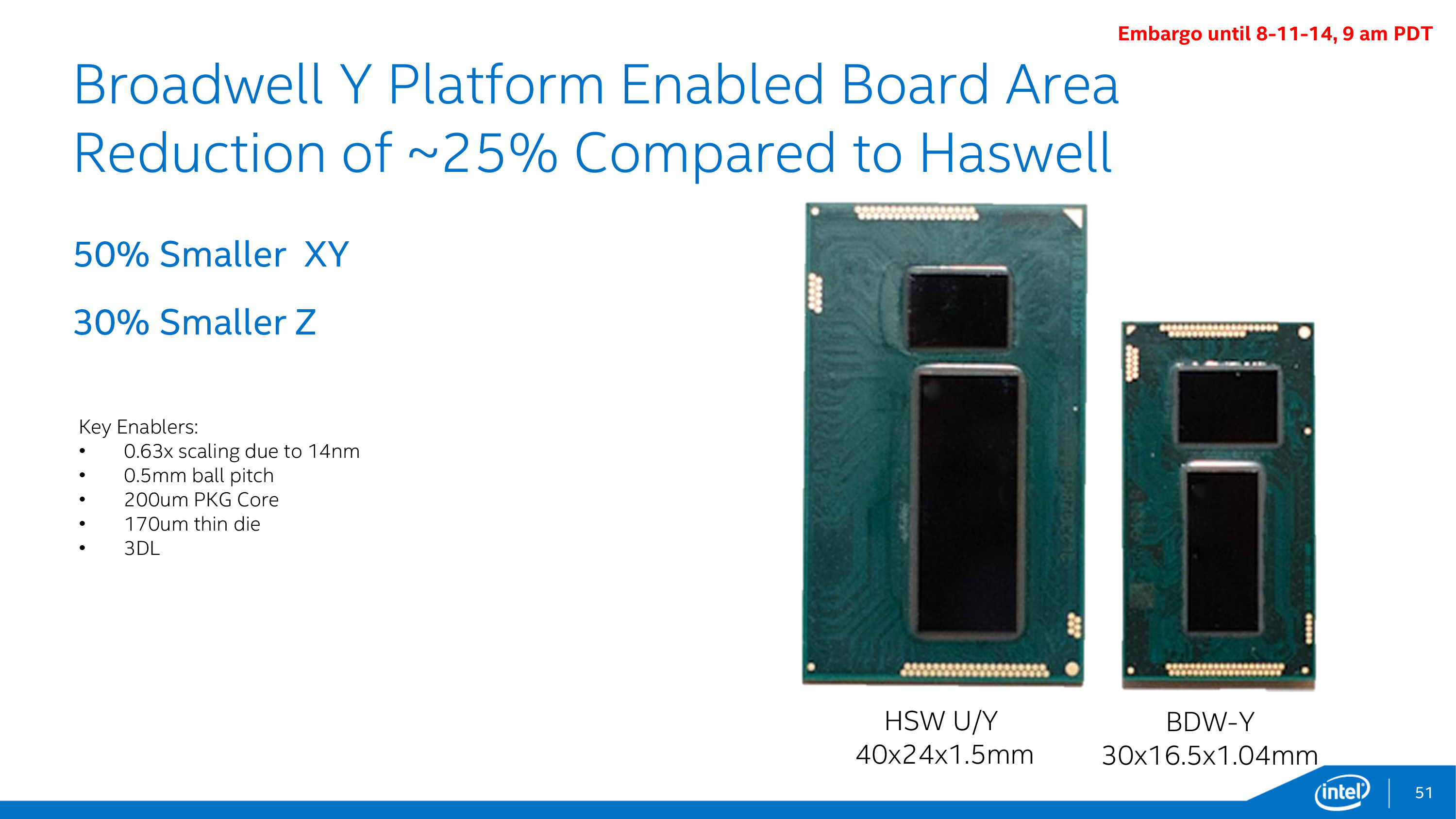
As was the case with power, reducing the size of Broadwell-Y is a multi-faceted effort. The 14nm process plays a big part here, allowing for one of the smallest Core CPU dice yet. At 82mm2 the Broadwell-Y CPU die is some 37% smaller than the Haswell-Y CPU die, none the less packing a dual-core CPU and a full GPU slice.
With such a small die Intel was in turn able to reduce the size of the entire SoC package through the combination of the reduced die area and further optimizations to the packaging itself. Haswell-Y’s already small ball pitch of .65mm was further reduced to just .5mm, producing a package with Intel’s smallest solder ball pads yet. Intel considers the reduction in the ball pitch to be the key change that allowed Broadwell-Y to be so small, as they were already pad-limited on Haswell-Y despite having ample excess packaging even after taking the CPU die’s larger size into account. As a result Broadwell-Y takes up almost 50% less surface area (XY) than Haswell-Y.
Intel has also made a number of changes for Broadwell-Y to reduce the Z-height of the Y SoCs, as even 1.5mm for the SoC starts to become a significant design constraint in a sub-10mm device. Again owing to the 14nm process, the Z-height of the Broadwell-Y die itself is down to 170um. Meanwhile the Z-height of the substrate has been cut in half from 400um to 200um, which accounts for nearly half of the total reduction in SoC Z-height.
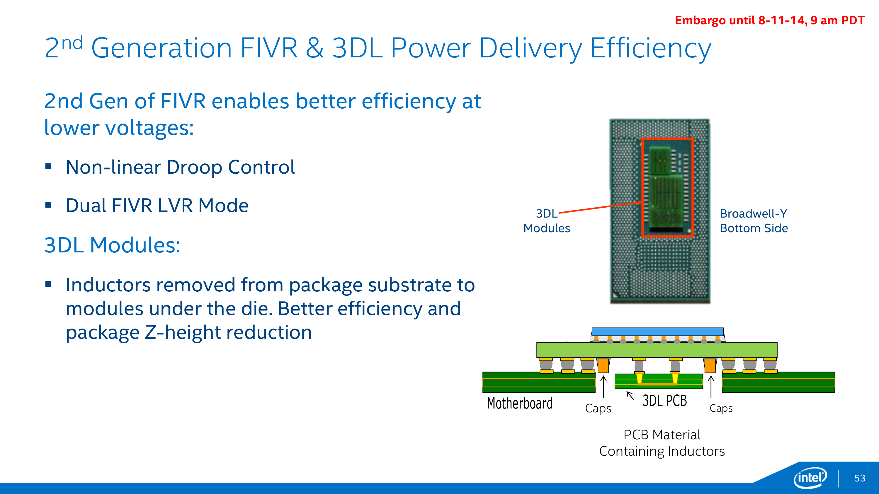
The final element in reducing the SoC Z-height, and what’s likely the most unorthodox change for Broadwell-Y’s packaging, is Intel’s 3DL inductors. The 3DLs aren’t just to improve energy efficiency as we discussed before, but they are part of Intel’s efforts to reduce the SoC size. For Broadwell-Y the 3DLs are on their own PCB on the back of the SoC, extending well below the back of the package. To accommodate this, logic boards housing Broadwell-Y will have a hole in them where the 3DL PCB would be in order to allow the complete SoC to fit. Because there are no BGA connections here this change isn’t quite as radical as it first appears, but it’s a very good example of just what lengths Intel was willing to go to reduce the package Z-height.
All told then, the combination of these space optimizations has reduced Broadwell-Y’s Z-height by nearly 30%, from 1.5mm on Haswell-Y to 1.04mm on Broadwell-Y (3DL PCB not included). By bringing Broadwell-Y’s thickness under 1.1mm, the SoC is now no taller than the other common components on a logic board (e.g. RAM), meaning the SoC will no longer stick out above the other components, which is useful both for saving space and for allowing simpler (flatter) heatsinks.
Finally, the smaller size of the Broadwell-Y package will also have a knock-on effect on the size of the logic board, further feeding into Intel’s goals to get Broadwell-Y into smaller devices. Intel tells us that the size of a complete platform (logic) board for Broadwell-Y has been reduced by roughly 25% as compared to Haswell-Y, allowing Broadwell-Y to better fit into not just thinner devices but overall smaller devices too.


158 Comments
View All Comments
psyq321 - Tuesday, August 12, 2014 - link
I also fail to see how will Intel be able to keep their cadence with Skylake without either skipping the entire generation (obsoleting it in 6 months does not sound reasonable from the financial point of view) or delaying the Skylake introduction.Also the fact that Intel decided to enable all 18 cores in the Haswell EP is telling IMHO. Initially, this was to happen only with BDW-EP, so it might not be impossible that Intel might just skip Broadwell for some segments and go with Skylake.
isa - Tuesday, August 12, 2014 - link
Those who know ain't talking, but I can observe the following;- Delaying Skylake for financial reasons related to Broadwell is braindead. Broadwell development costs are sunk costs and Intel is or should be trying to maximize overall profits, not just a particular program's profits. Intel should release Skylake as quickly as possible when its yields hit target values, regardless of Broadwell delays, with two caveats:
- If the Broadwell yield difficulties also slowed down Skylake, then Skylake will likely be inherently delayed to some degree
- If Intel screws up product planning such that they flood the market with Broadwell, then their customers might be very angry if they are stuck with that inventory upon a Skylake release.
My bet at this point? Broadwell H mobile will be a very short-lived product (about 6 months).
Krysto - Tuesday, August 12, 2014 - link
Definitely not Y or U, and wouldn't get M either. Whatever is above that.mczak - Monday, August 11, 2014 - link
For the gpu It is noteworthy that unlike nvidia and amd the subslice block (at least before gen8) doesn't really have an inherent minimal size which cannot be changed without significantly altering the architecture. E.g. Gen7 (which is just about the same as Gen7.5) had subslice sizes of 6 (IvyBridge GT1), 8 (IvyBridge GT2) and 4 even (BayTrail).It is also quite interesting that everybody (nvidia since gk2xx and Maxwell, amd since even before GCN, notably their Northern Islands VLIW4 designs, intel since Gen8) now has ended up with the exact same ALU:TEX ratio (one quad tmu per 64 ALU lanes), though of course the capabilities of these tmus vary a bit (e.g. nvidia can do fullspeed fp16 filtering, amd only half speed etc.)
tuxRoller - Monday, August 11, 2014 - link
http://www.phoronix.com/scan.php?page=article&...In the fourth to last paragraph an intel driver dev says that broadwell graphics "dwarf any other silicon iteration during my tenure, and certainly can compete with the likes of the gen3->gen4 changes."
I'm going to go with the guy who's actually developing the drivers on this.
AnnonymousCoward - Tuesday, August 12, 2014 - link
Simple question: will all the new Intel desktop CPUs have integrated graphics? If the answer's yes, why would they waste the silicon area for those using discrete?name99 - Tuesday, August 12, 2014 - link
Because the people who obsess about discrete graphics are a RIDICULOUSLY small fraction of the purchasing public, a fraction which is utterly unwilling to accept this fact and the fact that CPU design is not targeted at the needs of high-end gamers.wintermute000 - Tuesday, August 12, 2014 - link
"Because the people who obsess about discrete graphics are a RIDICULOUSLY small fraction of the purchasing public"Maybe not obsess, but to characterise the PC gaming market as ridiculously small, is pretty far off the mark....
DanNeely - Tuesday, August 12, 2014 - link
Compared to the total Intel CPU market and compared to the cost of creating an IGPless CPU die for the mainstream socket it's entirely on the mark. If you want an IGPless design your only choice is to wait a year for the Xeon derived LGA2011 model; and the fact that LGA1366 launched as an enthusiast design well before the Xeon's did, but that Intel hasn't done the same for any other models shows that it didn't sell well enough to justify rushing one for us.C'DaleRider - Tuesday, August 12, 2014 - link
Small fraction is right. Projected worldwide PC hardware sales for 2015 is ~ $385B (Source: eTForcasts). Projected PC gaming sales (both hardware and software) is ~$20B (Source: Statista), less than 10% of total PC hardware sales alone. A 10% market niche is very, very small in the overall scheme of the PC market.