Intel Broadwell Architecture Preview: A Glimpse into Core M
by Ryan Smith on August 11, 2014 12:01 PM ESTBroadwell GPU Architecture
While Intel’s tick products are relatively conservative on the CPU side, the same cannot be said for the GPU side. Although the same general tick-tock rules apply to GPUs as well as they do CPUs – the bigger architectural changes are on the tock – the embarrassingly parallel nature of graphics coupled with the density improvements from newer process nodes means that even in a tick Intel’s GPU improvements are going to be substantial. And Broadwell will be no exception.
From a high level overview, Broadwell’s GPU is a continuation of the Intel Gen7 architecture first pioneered in Ivy Bridge and further refined for Gen7.5 in Haswell. While there are some important underlying changes that we’ll get to in a moment, at a fundamental level this is still the same GPU architecture that we’ve seen from Intel for the last two generations, just with more features, more polish, and more optimizations than ever before.
In terms of functionality Broadwell’s GPU has been upgraded to support the latest and greatest graphics APIs, an important milestone for Intel as this means their iGPU is now at feature parity with iGPUs and dGPUs from AMD and NVIDIA. With support for Direct3D feature level 11_2 and Intel’s previous commitment to Direct3D 12, Intel no longer trails AMD and NVIDIA in base features; in fact with FL 11_2 support they’re even technically ahead of NVIDIA’s FL 11_0 Kepler and Maxwell architectures. FL 11_2 is a rather minor update in the long run, but support for it means that Intel now supports tiled resources and pre-compiled shader headers.
Meanwhile on the compute front, Intel has confirmed that Broadwell’s GPU will offer support for OpenCL 2.0, including OpenCL’s shared virtual memory. OpenCL 2.0 will bring with it several improvements that allow GPUs to be more robust compute devices, and though Intel doesn’t have a programming paradigm comparable to AMD’s HSA, SVM none the less affords Intel and OpenCL programmers the chance to better leverage Broadwell’s CPU and GPU together by directly sharing complex data structures rather than copying them around.
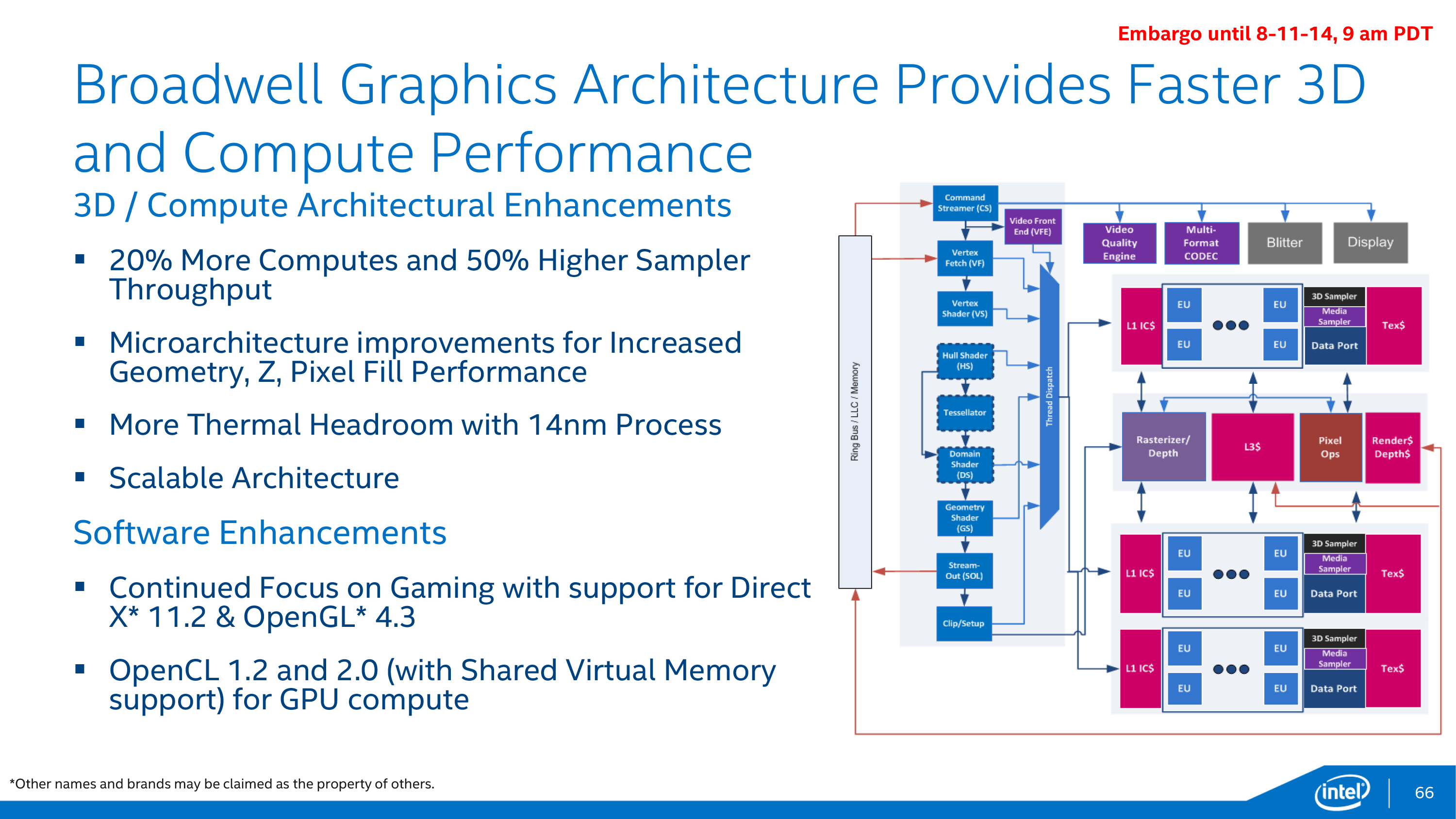
Digging deeper however quickly exposes that Intel hasn’t left their GPU architecture entirely alone. Broadwell-Y, like Haswell-Y before it, implements a single slice configuration of Intel’s GPU architecture. However the composition of a slice will be changing for Broadwell, and this will have a significant impact on the balance between various execution units.
| Low Level Architecture Comparison | |||||||||||||||||
| AMD GCN | NVIDIA Maxwell | Intel Gen7.5 Graphics | Intel Gen8 Graphics | ||||||||||||||
| Building Block | GCN Compute Unit | Maxwell SMM | Sub-Slice | Sub-Slice | |||||||||||||
| Shader Building Block | 16-wide Vector SIMD | 32-wide Vector SIMD | 2 x 4-wide Vector SIMD | 2 x 4-wide Vector SIMD | |||||||||||||
| Smallest Implementation | 4 SIMDs | 4 SIMDs | 10 SIMDs | 8 SIMDs | |||||||||||||
| Smallest Implementation (ALUs) | 64 | 128 | 80 | 64 | |||||||||||||
In Haswell-Y Intel used a GT2 configuration, which was composed of a single slice that in turn contained 2 sub-slices. In Intel’s GPU architecture the sub-slice is the smallest functional building block of the GPU, containing the EUs (shaders) along with caches and texture/data/media samplers. Each EU in turn was composed of 2 4-wide vector SIMDs, with 10 EUs per sub-slice.
For Broadwell Intel is not changing the fundamental GPU architecture, but they are rebalancing the number of EUs per sub-slice and increasing the number of sub-slices overall. As compared to Haswell, Broadwell’s sub-slices will contain 8 EUs per sub-slice, with a complete slice now containing 3 sub-slices. Taken altogether this means that whereas Haswell-Y was a 2x10EU GPU, Broadwell-Y will be a 3x8EU GPU.
The ramifications of this is that not only is the total number of EUs increased by 20% from 20 to 24, but Intel has greatly increased the ratio of L1 cache and samplers relative to EUs. There is now 25% more sampling throughput per EU, with a total increase in sampler throughput (at identical clockspeeds) of 50%. By PC GPU standards increases in the ratio of samplers to EUs is very rare, with most designs decreasing that ratio over the years. The fact that Intel is increasing this ratio is a strong sign that Haswell’s balance may have been suboptimal for modern workloads, lacking enough sampler throughput to keep up with its shaders.
Moving on, along with the sub-slices front end and common slice are also receiving their own improvements. The common slice – responsible for housing the ROPs, rasterizer, and a port for the L3 cache – is receiving some microarchitecture improvements to further increase pixel and Z fill rates. Meanwhile the front end’s geometry units are also being beefed up to increase geometry throughput at that end.
Much like overall CPU performance, Intel isn’t talking about overall GPU performance at this time. Between the 20% increase in shading resources and 50% increase in sampling resources Broadwell’s GPU should deliver some strong performance gains, though it seems unlikely that it will be on the order of a full generational gain (e.g. catching up to Haswell GT3). What Intel is doing however is reiterating the benefits of their 14nm process in this case, noting that because 14nm significantly reduces GPU power consumption it will allow for more thermal headroom, which should further improve both burst and sustained GPU performance in TDP-limited scenarios relative to Haswell.
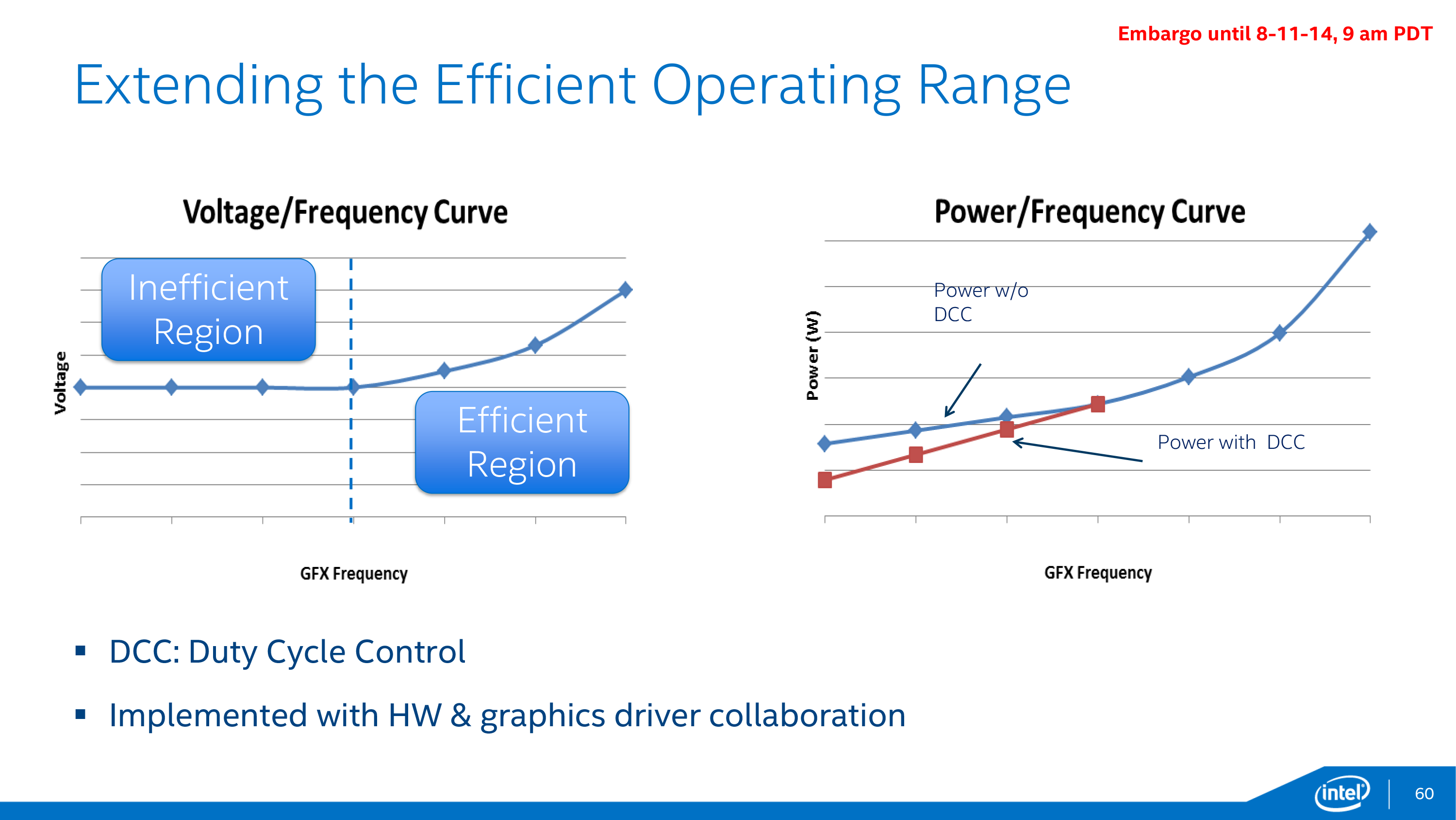
14nm isn’t the only technique Intel has to optimize power consumption on Broadwell’s GPU, which brings us to Broadwell’s final GPU technology improvement: Duty Cycle Control. While Intel has been able to clamp down on GPU idle power consumption over the years, they are increasingly fighting the laws of physics in extracting more idle power gains. At this point Intel can significantly scale down the frequency and operating voltage of their GPU, but past a point this offers diminishing returns. Transistors require a minimum voltage to operate – the threshold voltage – which means that after a certain point Intel can no longer scale down their voltage (and hence idle power consumption) further.
Intel’s solution to this problem is both a bit brute force and a bit genius, and is definitely unlike anything else we’ve seen on PC GPUs thus far. Since Intel can’t reduce their idle voltage they are going to start outright turning off the GPU instead; the process of duty cycling. By putting the GPU on a duty cycle Intel can run the GPU for just a fraction of the time – down to 12.5% of the time – which gets around the threshold voltage issue entirely.
This duty cycling is transparent to applications and the end user, with the display controller decoupled from the GPU clock domain and always staying online so that attached displays are always being fed regardless of what the GPU itself is doing. Control of the duty cycle is then handled through a combination of the GPU hardware and Intel’s graphics drivers, so both components will play a part in establishing the cycle.
Because today’s preview is Broadwell-Y centric, it’s unclear whether GPU duty cycle control is just a Broadwell-Y feature or whether it will be enabled in additional Broadwell products. Like many of Intel’s announced optimizations for Broadwell, duty cycle control is especially important for the TDP and battery life constrained Y SKU, but ultimately all mobile SKUs would stand to benefit from this feature. So it will be interesting to see just how widely it is enabled.

Moving on, last but not least in our GPU discussion, Intel is also upgrading their GPU’s media capabilities for Broadwell. The aforementioned increase in sub-slices and the resulting increase in samplers will have a direct impact on the GPU’s video processing capabilities – the Video Quality Engine and QuickSync – further increasing the throughput of each of them, up to 2x in the case of the video engine. Intel is also promising quality improvements in QuickSync, though they haven’t specified whether this is from technical improvements to the encoder or having more GPU resources to work with.
Broadwell’s video decode capabilities will also be increasing compared to Haswell. On top of Intel’s existing codec support, Broadwell will be implementing a hybrid H.265 decoder, allowing Broadwell to decode the next-generation video codec in hardware, but not with the same degree of power efficiency as H.264 today. In this hybrid setup Intel will be utilizing both portions of their fixed function video decoder and executing decoding steps on their shaders in order to offer complete H.265 decoding. The use of the shaders for part of the decoding process is less power efficient than doing everything in fixed function hardware but it’s better than the even less optimal CPU.
The use of a hybrid approach is essentially a stop-gap solution to the problem – the lead time on the finalization of H.265 would leave little time to develop a fixed function encoder for anyone with a long product cycle like Intel – and we expect that future generation products will have a full fixed function decoder. In the meantime Intel will be in the company of other GPU manufacturers such as NVIDIA, who is using a similar hybrid approach for H.265 on their Maxwell architecture.
Finally, Broadwell’s display controller will be receiving an update of its own. Broadwell is too soon for HDMI 2.0 or DisplayPort 2.0 – it will support HDMI 1.4 and DP 1.2/eDP 1.3a respectively – but the Y SKU in particular is getting native support for 4K. This is admittedly something of a backport since Haswell already supports 4K displays, but in Haswell’s case that feature was not available on Haswell-Y, so this is the first time native 4K support has come to a Y series SKU. This means that Broadwell-Y will be able to drive 4K displays, whether that means a 4K display in the device itself, or a 4K display hooked up internally (with an overall limit of 2 displays on Broadwell-Y). Don’t expect Broadwell-Y to have the performance necessary to do intensive rendering at this resolution, but for desktop work and video playback this should be enough.


158 Comments
View All Comments
psyq321 - Tuesday, August 12, 2014 - link
Actually, apart from power-users I fail to see any tangible improvements in performance of modern CPUs that matter to desktop/notebook usage, Intel or otherwise.In the mobile space, it is improvements in GPU which mattered, but even that will eventually flatten once some peak is reached since graphics improvements on 4" / 5" screen can only matter to wide audiences up to some point.
However, there are surely enough customers that do look forward to more power - this is workstation and server market. Skylake and its AVX512 will matter to scientists and its enormous core count in EP (Xeon) version will matter to companies (virtualization, etc.).
Standard desktop, not so much. But, then again, ever since Core 2 Quad 6600 this was the case. If anything, large-scale adoption of SSDs is probably the single most important jump in desktop performance since the days of Conroe.
Khenglish - Monday, August 11, 2014 - link
I find the reduction in die thickness to be a big deal. Maybe this will prevent temperatures from getting out of control when the cpu core area gets cut in half for 14nm. High power 22nm cpus already easily hit 30c temperature difference between the cpu and heatsink.AnnonymousCoward - Tuesday, August 12, 2014 - link
Probably not. I'd guess thermal dissipation is the same.dgingeri - Monday, August 11, 2014 - link
PC sales are down mostly because people can keep their systems longer due to the lack of innovation coming from Intel on desktop chips and the lack of utilizing the current CPU technology by software developers. They could be so much more, if only developers would actually make use of the desktop CPU capabilities for things such as a voice command OS that doesn't need to be trained. Intel would then have a reason to produce more powerful chips that would trigger more PC sales.As it is, the current processor generation is less than 10% faster clock for clock compared to three generations ago. A great many thing aren't any faster at all. Know what? It doesn't even matter because nothing uses that much power these days.
Tablets and smartphones can't take the place of full PCs for most people. Their screens are just too small. Perhaps the younger generations prefer the small form factors right now, but give them a little time, and their eyes won't let them use such things. I can see the move to laptops, especially with 14-15" screens, but trying to show the same content on a 10" screen is just near unusable, and a 5" smartphone screen is just downright impossible. However, desktop PCs still have their place, and that's never going to change.
This push by "investors" for the tablet and smartphone market is just asinine. Broadwell isn't going to help sales all that much. Perhaps, they might sell some more Intel based tablets, but it won't be all that much of an improvement. Tablets have a niche, but it really isn't that much of one.
HanzNFranzen - Monday, August 11, 2014 - link
Tablets are a niche and not much of one? lol yea ok... well while you were asleep in a cave, over 195 million tablets were sold in 2013 between Android/Apple/Microsoft which is just shy of 80 million more than the previous year. World wide PC sales totaled 316M units, so we are talking nearly 2 tablets for every 3 PC's sold. Eh...small niche...dgingeri - Monday, August 11, 2014 - link
yeah, lots of people have them, but how much do they really use them? I have two, one Android and one Windows RT, and I only use them for reading books or for reading the web news while away from home. The Windows unit showed promise, since I could use it to run Office and terminal programs, but I ended up not using it at work anymore because it couldn't use a USB to serial adapter for talking to switches and raid arrays. It ended up being only half useful. They're nice to have for certain things, but they aren't as versatile as a PC. My parents own two, and two PCs, and they use the PCs far more. My older sister has one, and she barely uses it. Her 7 year old uses it to play games most of the time. My nephew has one, and he's only ever used it to read Facebook. It's a telling tale that everyone I've known who has one only has limited used for it.mapesdhs - Monday, August 11, 2014 - link
Point taken, but if people are *buying* them, irrespective of whether they use them,then it doesn't really matter.
Besides, this whole field of mobile computing, smart phones, tablets, now phablets,
etc., it's too soon to be sure where we're heading long-term.
Many people say the copout porting of console games to PCs with little enhancement
is one thing that's harmed PC gaming sales. This may well be true. Now that the newer
consoles use PC tech more directly, perhaps this will be less of an issue, but it's always
down to the developer whether they choose to make a PC release capable of exploiting
what a PC can do re high res, better detail, etc. Wouldn't surprise me if this issue causes
internal pressures, eg. make the PC version too much better and it might harm console
version sales - with devs no doubt eager to maximise returns, that's something they'd
likely want to avoid.
Ian.
az_ - Monday, August 11, 2014 - link
Ryan, could you add a size comparison to an ARM SOC that would be used in a tablet? I wonder how close are Intel in size. Thanks.name99 - Tuesday, August 12, 2014 - link
BDW-Y is 82 mm^2. The PCH looks like it's about a third of that, so total is maybe 115 mm^2 or so.In comparison, Apple A7 is about 100 mm^2.
A7 includes some stuff BDW-Y doesn't, and vice versa, so let's call it a wash in terms of non-CPU functionality.
BDW-Y obviously can perform a LOT better (if it's given enough power, probably performs about the same at the same power budget). On the other hand it probably costs about 10x what an A7 costs.
Krysto - Tuesday, August 12, 2014 - link
Sure, also let's conveniently forget that Broadwell Y benefits not only of 3D transistors, but a 2 generation node shrink, too, compared to A7. Now put A7 on 14nm and 3d transistors...and let's see which does better.This is the issue nobody seems to understand, not even Anand, or just conveniently ignored it when he declared that the "x86 myth is busted". At the time we were talking about a 22nm Trigate Atom vs 28nm planar ARM chip, with Atom barely competing on performance (while costing 2x more, and having half the GPU performance). Yet Anand said the x86 bloat myth is busted...How exactly?! Put them on the same process technology...and then we'll see if x86 myth is indeed busted, or it's still bloated as a pig.