Imagination's PowerVR Rogue Architecture Explored
by Ryan Smith on February 24, 2014 3:00 AM EST- Posted in
- GPUs
- Imagination Technologies
- PowerVR
- PowerVR Series6
- SoCs
Background: How GPUs Work
Seeing as how this is our first in-depth architecture article on a SoC GPU design (specifically as opposed to PC-derived designs like Intel and NVIDIA), we felt it best to start at the beginning. For our regular GPU readers the following should be redundant, but if you’ve ever wanted to learn a bit more about how a GPU works, this is your place to start.
GPUs, like most complex processors, are composed of a number of different functional units responsible for the different aspects of computation and rendering. We have functional units that setup geometry data, frequently called geometry engine, geometry processors, or polymorph engines. We have memory subsystems that provide caching and access to external memory. We have rendering backends (ROPs or pixel co-processors) that take computed geometry and pixels to blend them and finalize them. We have texture mapping units (TMUs) that fetch textures and texels to place them within a scene. And of course we have shaders, the compute cores that do much of the heavy lifting in today’s games.
Perhaps the most basic question even from a simple summary of the functional units in a GPU is why there are so many different functional units in the first place. While conceptually virtually all of these steps (except memory) can be done in software – and hence done in something like a shader – GPU designers don’t do that for performance and power reasons. So-called fixed function hardware (such as ROPs) exists because it’s far more efficient to do certain tasks with hardware that is tightly optimized for the job, rather than doing it with flexible hardware such as shaders. For a given task flexible hardware is bigger and consumes more power than fixed function hardware, hence the need to do as much work in power/space efficient fixed function hardware as is possible. As such the portions of the rendering process that need flexibility will take place in shaders, while other aspects that are by their nature consistent and fixed take place in fixed function units.
The bulk of the information Imagination is sharing with us today is with respect to shaders, so that’s what we’ll focus on today. On a die area basis and power basis the shader blocks are the biggest contributors to rendering. Though every functional unit is important for its job, it’s in the shaders that most of the work takes place for rendering, and the proportion of that work that is bottlenecked by shaders increases with every year and with every generation, as increasingly complex shader programs are created.
So with that in mind, let’s start with a simple question: just what is a shader?
At its most fundamental level, a shader core is a flexible mathematics pipeline; it is a single computational resource that accepts instructions (a shader program) and executes it in order to manipulate the pixels and polygon vertices within a scene. An individual shader core goes by many names depending on who makes it: AMD has Stream Processors, NVIDIA has CUDA cores, and Imagination has Pipelines. At the same time how a shader core is built and configured depends on the architecture and its design goals, so while there are always similarities it is rare that shader cores are identical.
On a lower technical level, a shader core itself contains several elements. It contains decoders, dispatchers, operand collectors, results collectors, and more. But the single most important element, and the element we’re typically fixated on, is the Arithmetic Logic Unit (ALU). ALUs are the most fundamental building blocks in a GPU, and are the base unit that actually performs the mathematical operations called for as part of a shader program.
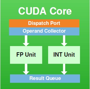
An NVIDIA CUDA Core
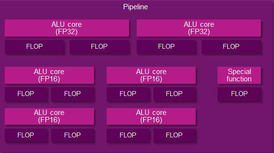
And an Imgination PVR Rogue Series 6XT Pipeline
The number of ALUs within a shader core in turn depends on the design of the shader core. To use NVIDIA as an example again, they have 2 ALUs – an FP32 floating point ALU and an integer ALU – either of which is in operation as a shader program requires. In other designs such as Imagination’s Rogue Series 6XT, a single shader core can have up to 7 ALUs, in which multiple ALUs can be used simultaneously. From a practical perspective we typically count shader cores when discussing architectures, but it is at times important to remember that the number of ALUs within a shader core can vary.
When it comes to shader cores, GPU designs will implement hundreds and up to thousands of these shader cores. Graphics rendering is what we call an embarrassingly parallel process, as there are potentially millions of pixels in a scene, most of which can be operated in in a semi-independent or fully-independent manner. As a result a GPU will implement a large number of shader cores to work on multiple pixels in parallel. The use of a “wide” design is well suited for graphics rendering as it allows each shader core to be clocked relatively low, saving power while achieving work in bulk. A shader core may only operate at a few hundred megahertz, but because there are so many of them the aggregate throughput of a GPU can be enormous, which is just what we need for graphics rendering (and some classes of compute workloads, as it turns out).
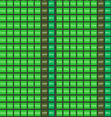
A collection of Kepler CUDA cores, 192 in all
The final piece of the puzzle then is how these shader cores are organized. Like all processors, the shader cores in a GPU are fed by a “thread” of instructions, one instruction following another until all the necessary operations are complete for that program. In terms of shader organization there is a tradeoff between just how independent a shader core is, and how much space/power it takes up. In a perfectly ideal scenario, each and every shader core would be fully independent, potentially working on something entirely different than any of its neighbors. But in the real world we do not do that because it is space and power inefficient, and as it turns out it’s unnecessary.
Neighboring pixels may be independent – that is, their outcome doesn’t depend on the outcome of their neighbors – but in rendering a scene, most of the time we’re going to be applying the same operations to large groups of pixels. So rather than grant the shader cores true independence, they are grouped up together for the purpose of having all of them executing threads out of the same collection of threads. This setup is power and space efficient as the collection of shader cores take up less power and less space since they don’t need the intelligence to operate completely independently of each other.

The flow of threads within a wavefront/warp
Not unlike the construction of a shader core, how shader cores are grouped together will depend on the design. The most common groupings are either 16 or 32 shader cores. Smaller groupings are more performance efficient (you have fewer shader cores sitting idle if you can’t fill all of them with identical threads), while larger groupings are more space/power efficient since you can group more shader cores together under the control of a single instruction scheduler.
Finally, these groupings of threads can go by several different names. NVIDIA uses the term warp, AMD uses the term wavefront, and the official OpenGL terminology is the workgroup. Workgroup is technically the most accurate term, however it’s also the most ambiguous; lots of things in the world are called workgroups. Imagination doesn’t have an official name for their workgroups, so our preference is to stick with the term wavefront, since its more limited use makes it easier to pick up on the context of the discussion.
Summing things up then, we have ALUs, the most basic building block in a GPU shader design. From those ALUs we build up a shader core, and then we group those shader cores into a array of (typically) 16 or 32 shader cores. Finally, those arrays are fed threads of instructions, one thread per shader core, which like the shader cores are grouped together. We call these thread groups wavefronts.
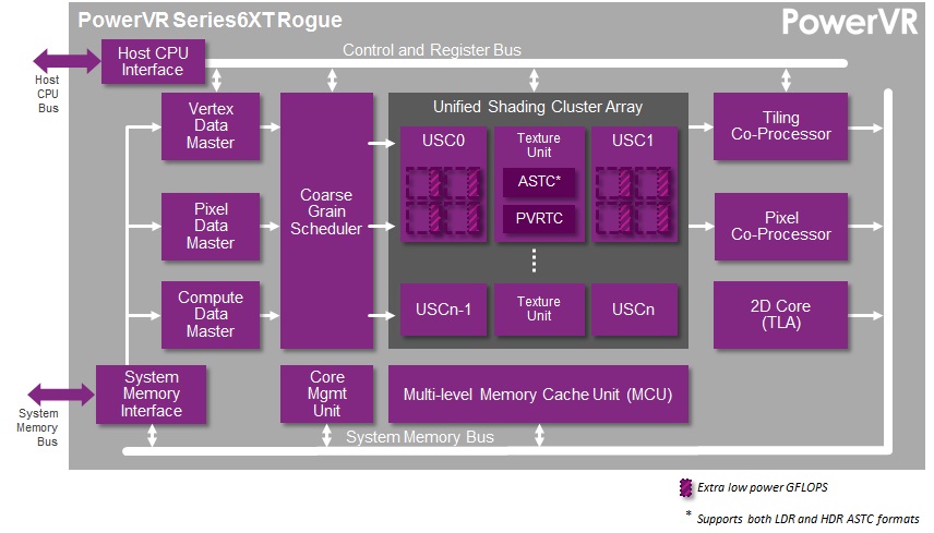
And with that behind us, we can now take a look at the PowerVR Series 6/6XT Unfied Shading Cluster.


95 Comments
View All Comments
grahaman27 - Monday, February 24, 2014 - link
Because apple can't have all the cool stuff!CiccioB - Monday, February 24, 2014 - link
Architecture wise, PowerVR seems more alike AMD's VLIW then nvidia's Kepler (or G200 or Fermi or Maxwell).That means PowerVR is going to have the same issues AMD had with VLIW and general computing performances and ILP.
There are also many interesting facts that could be analysed:
1. AMD went from having 5 computing ALUs to 4 to improve efficiency before switching to a completely new architetecture (CGN). PowerVR went from 5 to 7 ALUs (if we consider them all as separate units, are you sure it can process 16bit instructions togheter with 32bits one and not that those 32bits units can each execute 2x16bits instructions alternatively?)
2. PowerVR is using the same marketing politics used by AMD to count their computing core. They showed they had more computing core than nvidia competitor's architecture, but in the end, for the fact that they couldn't keep all of them feeded, they were less efficient.
3. nvidia passing from Kepler desktop to Kepler mobile removed ROPs and TMU. So, probably they think their architetcure (and GPUs on mobile in general) are less bottlenecked under those terms. PowerVR went incresing them, so they possibly think ROPs and TMU are more important then shaders... which is which? Both of them are trying to hide some deficiency of their respective architetcture?
4. We do not really know anything about PowerVR geometry power. nvidia in Kepler SMX has special function units (polymorph engine) that is connected directly to the shaders. That seems to give a enormous boost to geometric performaces (expecially tesselation) that rightly scale with the number of active SMX. PowerVR seems to have chosen AMD implementation with off-computational-core tesselator that do not scale automatically. How's going to behave PowerVR with future games that may need more geometric performances?
5. Again, as someone altready asked, tile based rendering was used on the desktop but was soon abandoned as it could not give any real advantages over the raw power of other architectures that grew much faster that what PowerVR could optimize their algorithms, making tile based rendering less and less profitable. What makes that scenario different that what we are witnessing in this period where mobile resolutions are growing to be even bigger than desktop monitors and that games complexity is gonig to increase for the arrival of these really powerful GPUs (K1 in primis)?
6. We lack the die area occupation comparison. How big is a 6 modules Rogue with respect to nvidia K1? If it is, just to say, twice nvidia die area, that would be a problem even thought the power consumption is the same. If it half, that would mean that PowerVR could make double K1 perfomance (if we believe Rogue 192 shaders perform like Kepler 192 ones). That would mean nvidia is in trouble just before beginning the high end socket race.
7. It seems PowerVR is behaving a bit like 3DFx did at the time, till it died. They were using their advanced but old technology to the exterme, so they rendered at 16bit instead of 32, used 16bit Zbuffer instead of 24 and many more "tricks" that were forced to try to hide what was quite clear: 3DFX didn't have the right architecture to compete with new companies like nvidia and ATI that started their story with the right step and much more powerful architectures (TNT2 simply destroyed Voodoo3 under all points, and beware, I was an Voodoo3 unfortunate owner). Will PowerVR go the same end trying to force the use of obsolete technics while all the others competitors are clearly pointing to constantly increasing raw power with no trade-offs (or with minimal ones?)
DanNeely - Monday, February 24, 2014 - link
AMDs shift from VLIW5 to VLIW4 was driven by the decline of DX9. DX9 was explicitly designed around a 5 step path; VLIW5 was tied directly to that. DX10's more flexible workflow rarely allowed for a 5 wide execution path.For VLIW4 AMD tied functional units together more than Imagination appears to've done here. They have 4 normal ALUs that match with the 4x 16bit ALUs in Rouge; but to do a special function operation they used 3 of the 32bit ALUs instead of using dedicated hardware. The tradeoff was that a special function cost a lot more normal processing capacity than it did before. Power VR doesn't appear to have put enough general purpose computing power place to do the same, and is required to use a dedicated SFU by default (even assuming they felt the tradeoff was worth like AMD does).
The main thing I'm curious about is if the 16 and 32bit ALUs are separate hardware; or if they implemented them similar to how SSE/AVX are done on x86 where the same hardware can do 2 32 (16) bit or 1 64 (32) bit operation.
http://www.anandtech.com/show/4061/amds-radeon-hd-...
Ryan Smith - Monday, February 24, 2014 - link
"The main thing I'm curious about is if the 16 and 32bit ALUs are separate hardware; or if they implemented them similar to how SSE/AVX are done on x86 where the same hardware can do 2 32 (16) bit or 1 64 (32) bit operation."They're separate hardware. Just as how NVIDIA uses separate FP32 and FP64 CUDA cores.
ryszu - Monday, February 24, 2014 - link
We're nothing like VLIW4/5, mobile Kepler still has ROPs and texture hardware, the area is absolutely nowhere near where you think it is and the architectural features we have in the front-end remain class leading and entirely sensible for mobile.CiccioB - Monday, February 24, 2014 - link
Sorry, maybe I was not that clear. I didn't meant they removed completely ROPs and TMUs, I was hinting to the fact that they decreased their number in a SMSX for mobile with respect to a SMX for desktop. ROPs are tied to memory channel, and that may be the cause. But TMUs are not, so they could be the same number as they are in desktop implementation.It seems nvidia sees those many ROPs and TMUs bottlenecked by RAM bandwidth so they spare space and power by not adding them.
PowerVR on the contrary has a ROPs and TMUs ratio with respect to shaders (or computing core) that is much higher. One or the other took the wrong assumption (also tied to the memory controller width, that may be higher as you want but costs in terms of die size and power). I'm curious to know who made it.
ryszu - Monday, February 24, 2014 - link
Ah, I see. Our ALU:TEX:ROP is different to Kepler (and again to Maxwell), yes. We're focused on still being strong for the basics (texturing, pixel fill) while still having a lot of shading to go with it. I can't speak for NV's design choices, just that both have pros and cons depending on market.The rest of your comment still has a lot of problems in respect to the PowerVR Rogue architecture and how it works, how it works in mobile, and how it compares to K1 and pre-GCN AMD.
Ryan Smith - Monday, February 24, 2014 - link
"Architecture wise, PowerVR seems more alike AMD's VLIW then nvidia's Kepler (or G200 or Fermi or Maxwell).That means PowerVR is going to have the same issues AMD had with VLIW and general computing performances and ILP."
To be honest I had the same thought at first. We've known that Rogue has multiple slots per pipeline since the Apple A7 came out, so when I first heard that I had the same thought. Given the greater simplicity of mobile SoCs, it would certainly make sense.
That said, after finally having access to IMG's technical details, it's clear to me that this is not the case, which was part of the reason I was so excited to work on this article. It's sort of like Fermi and it's sort of like VLIW5, but in reality it's neither.
The most important point is that in AMD's VLIW designs they had 4/5 ALUs all alike (for the sake of this discussion we'll ignore the T-unit). So to maximize a Streaming Processor's utilization, you needed to be able to extract a full 4-5 instructions of ILP out of a thread. Which was easy to do under DX9 (RGBA + lighting) and a lot harder to do under DX10.
Rogue on the other hand doesn't have ILP requirements nearly as high due to the fact that the 6 ALUs are not identical and are rarely all going to be in use at once (we don't even count the FP16 units in our GFLOPs calculations). They do have ILP requirements, unlike GCN, but for FP32 it's only 2 instructions for the 2 FP32 ALUs. This is in fact rather similar to Kepler (but not Maxwell) in that NVIDIA has a similar reliance on ILP to keep all of their CUDA cores fed. Half of the threads on Kepler need to co-issue another FP32 op to fill the other 64 CUDA cores in an SMX; Rogue is a bit worse in this regard since every thread needs to co-issue to fill every second FP32 ALU.
FP16 on the other hand is trickier, since that's a full 4 ALU setup. Worst case scenario is that IMG needs to pull off 4 instructions of ILP to maximize their utilization, but this is a bit murkier since we don't know why Series 6 had the unusual 3 operator FP16 ALUs in the first place. As such I'm less familiar with where FP16 is being used in mobile today, so it's harder to draw comparisons for what FP16 utilization may be like. That said, there's also the unknown of die size and power requirements of using FP16 units for FP16 math versus using FP32 units for the same task. I'm not sure if IMG has reason to be worried about FP16 utilization if they can pack 2x as much hardware in the same die size and power envelope.
Ultimately I'd classify Rogue as being closer to Fermi/Kepler than VLIW, which is why those are the comparisons we went with in the article. The 2 wide FP32 pipeline isn't nearly as narrow as AMD's VLIW, and the instructions themselves aren't the inflexible chaos that was VLIW as a language.
"Again, as someone altready asked, tile based rendering was used on the desktop but was soon abandoned as it could not give any real advantages over the raw power of other architectures that grew much faster that what PowerVR could optimize their algorithms, making tile based rendering less and less profitable. What makes that scenario different that what we are witnessing in this period where mobile resolutions are growing to be even bigger than desktop monitors and that games complexity is gonig to increase for the arrival of these really powerful GPUs (K1 in primis)?"
One of the problems IMG faced in the old days was that DirectX and Windows weren't very well suited for their TBDR design; they pretty much had to fight the API at times to get what they wanted. For iOS/Android it's difficult to draw comparisons - though I'd note iOS has always been driven by IMG GPUs and hence always used TBDR - but Windows for its part has since gotten much better. In particular there are API hooks to allow applications to see if the GPU is TBDR. I'm not sure if that's enough, but it does mean things have changed at least a little bit since the old days.
Scali - Monday, February 24, 2014 - link
In D3D11 there is now a flag to indicate whether you are running on a TBDR device or not: http://msdn.microsoft.com/en-us/library/windows/de...CiccioB - Monday, February 24, 2014 - link
I didn't realize that in counting those GFlops you ignored the 16bit ALUs, Issuing two instructions should be much easier than issuing 3, 4 or even 5, not to speak about 6 or 7.However I bet that PowerVR next architecture (or the next one again) will remove those 16bit ALUs and will introduce a couple of them able to issue 32 OR 2x16bit instruction, so that they can pack more shaders in the same area.
About TBDR design... the alternative to DirectX is OpenGL. Is it more suited for TBDR architecture than "brute force" ones?
Still I perceive PowerVR architecture as something from the past that has survived to to now until the big one have entered the mobile game for real. Kepler is a very efficient architecture and Maxwell has demonstrated that it can be even better. How is PowerVR going to fight against an architecture as flexible as nvidia ones that can also be used for CUDA computing and thus being adopted into markets (and for other tasks) PowerVR cannot with their current architecture? Not to forget that nvidia can now easily bring to their mobile versions whatever engine exists for their desktop GPUs.
Will extreme (but not so flexible) efficiency win against something not that efficient but able to do much more things in a easier way?
Would mobile game engines bet more on computing shaders power or memory bandwidth?
Will new DX10/DX11-alike engines (whose features are supported by new architectures) still be TBDR friendly? Does TBDR design still scale for the modern ultra high resolution displays or as for desktops "brute force" (or simply more power more performance) will rule out?
I think this year will tell us very much.