Intel Z87 Motherboard Review with Haswell: Gigabyte, MSI, ASRock and ASUS
by Ian Cutress on June 27, 2013 8:00 AM EST- Posted in
- Motherboards
- Intel
- MSI
- Gigabyte
- ASRock
- Asus
- Haswell
- Z87
- Shark Bay
- Lynx Point
ASRock Z87 Extreme6/AC In The Box
As we are moving up into the $220 bracket with the Z87 Extreme6/AC, the package as a whole has to be a step above that of the $170 models. Not only in features, this means the box as well. For the ASRock motherboard, we get the following:
Driver CD
User Guide
Rear IO Panel
Front USB 3.0 Panel with SSD Holder
Rear Bracket for USB 3.0 Panel
802.11ac WiFi Antenna
Six SATA Cables
Rigid SLI Bridge
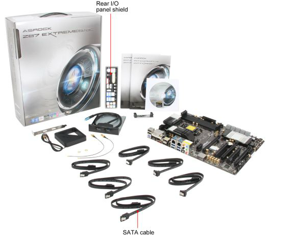
The addition of the USB 3.0 Front panel is always a plus – as we get three USB 3.0 headers onboard it makes sense to add in that front panel. The WiFi antenna is a new design although it essentially requires it to be suspended from somewhere to get best coverage. This is in comparison to the ASUS solutions in the past which are magnetic. The ASRock design does feel better than the last generation, but there is still room for improvement.
ASRock Z87 Extreme6/AC Overclocking
Experience with ASRock Z87 Extreme6/AC
On our last ASRock review, of the Z77 OC Formula, we had great fun playing around with all the overclock settings on what was an overclock-oriented motherboard. Due to the success of the OC Formula, ASRock are pushing some of the features down into the channel motherboards, especially when it comes to BIOS and automatic overclock options. In the OS, we get Performance Mode, Power Saving Mode and Auto Tuning, with the Power Saving mode being rather neat in exchange for some initial processing latency. The BIOS has some more typical options ranging from 4.0 GHz to 4.8 GHz in 200 MHz increments.
For manual adjustments, while ASRock’s software options have an upgrade to something more friendly, I am more a fan of their BIOS controls which are neatly laid out and easy to understand, with explanations on what each setting does. In terms of performance, we were unable to push the ASRock far because our engineering sample board had issues with the heatsinks. We have a retail sample in house, but have not had time to run the tests yet! We will update this page when we do so, but up until the point where the heatsink became an issue, the ASRock felt good rising up the MHz.
The only downside in our overclock testing was the lack of any form of reliable voltage monitoring tool. ASRock’s own software is configured incorrectly to report the VRIN voltage rather than VCore where it says ‘VCore Voltage:’, and other tools were stuck showing the stock voltage.
Methodology:
Our standard overclocking methodology is as follows. We select the automatic overclock options and test for stability with PovRay and OCCT to simulate high-end workloads. These stability tests aim to catch any immediate causes for memory or CPU errors.
For manual overclocks, based on the information gathered from previous testing, starts off at a nominal voltage and CPU multiplier, and the multiplier is increased until the stability tests are failed. The CPU voltage is increased gradually until the stability tests are passed, and the process repeated until the motherboard reduces the multiplier automatically (due to safety protocol) or the CPU temperature reaches a stupidly high level (100ºC+). Our test bed is not in a case, which should push overclocks higher with fresher (cooler) air.
Automatic Overclock:
For these automatic overclocks we were using a second i7-4770K CPU, which is a bit of a dog, failing to reach 4.2 GHz.
In the software, we are given three options: Performance Mode, Sandered (sic) Mode and Power Saving Mode. Selecting Performance Mode gives the additional option of Auto Tuning. In terms of OS options, we get an ‘Optimized CPU Setting’ from 4.0 GHz to 4.8 GHz in 200 MHz increments. Here are our results.
In Performance Mode, the system ran the CPU at the 39x multiplier no matter what the loading. This setting scored 1613.14 during PovRay and a peak temperature of 76C during PovRay.
In Power Saving Mode, the system runs at the 8x multiplier most of the time. When a constant load is applied, the system slowly ramps up the CPU speed in small jumps until it hits 39x – the process requires a full 8 seconds of loading to reach full speed. Due to the 8 seconds of ‘less-than-peak’ performance, the system scored 1524.34 during PovRay, and recorded a peak temperature of 76C during OCCT.
In Auto Tuning Mode, the system stress -tested the CPU speed at 3.0 GHz, and on a completed test raised the multiplier and started again. On this method, the system rose to 4.2 GHz and stopped, causing the system to run at 4.2 GHz during idle and at load. With this setting, the system scored 1736.67 during PovRay and recorded a peak temperature of 85C during OCCT.
Manual Overclock:
For our manual overclocks, the CPU used in the other motherboards was available for testing. Our manual overclock settings started with the system at 40x100, with the CPU voltage set at 1.000 volts, CPU VRIN set to 1.65 volts, and load line calibration at Level 1. On a successful stress test, the multiplier was raised and the test repeated; on a failed stress test, the voltage was increased by 0.025 volts and the test repeated.
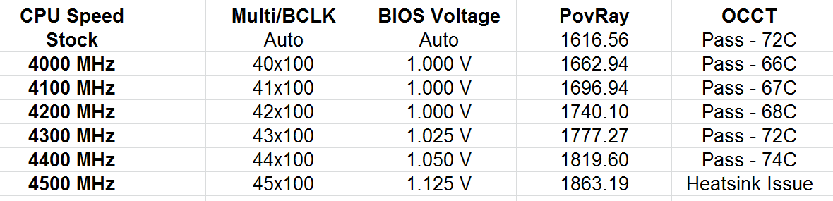
Unfortunately due to the VRM heatsink issue on our board with ES heatsinks, the system did not like any voltages over 1.100 volts, causing lockups. We have a retail sample in to test, but it arrived slightly too late for us to circle back around and retest before leaving for Computex. Watch this space, it will be updated soon.


58 Comments
View All Comments
clyman - Tuesday, November 26, 2013 - link
In my personal experience and from ASUS tech support, the safest way to update bios is by first downloading it. This mobo has an excellent update program in bios that only looks at local drives, not online. I found it quite simple at each bios update.silenceisgolden - Thursday, June 27, 2013 - link
Great job Ian, really looking forward to the super high end motherboard review as well! I'm curious though, did you use the VGA port at all in any of these reviews, and also when was the last time you used a VGA port?IanCutress - Thursday, June 27, 2013 - link
My Korean 1440p panels are all via DVI-D. But the VGA comes in use when you have to use a DVI-I to VGA converter for DVI-I cables. Otherwise you need a DVI-D cable.JeBarr - Thursday, June 27, 2013 - link
Great review Ian. I very much appreciate your taking the time to explain the PCIe slot assignment and repeating the less-than-x8-no-good-for-SLI truth that needs to spread far and wide.What I took away from this review when analysing my own usage patterns and component choices is that each of the boards in this review would be better suited to the mATX form factor. There is no point in purchasing these mid-high end boards for multi-GPU, multi-display configs. There are only a handful of full size z87 boards that in my opinion earn their full-size status.
Shadowmaster625 - Thursday, June 27, 2013 - link
If it has fully integrated voltage regulators then why in blazes does it still need $20 worth of components buried beneath $3 heatsinks surrounding the cpu socket? Yeah, that's what I thought....DanNeely - Thursday, June 27, 2013 - link
What FIVR means to Intel isn't quite what you think it means. What's on package is the collection of VRs needed to provide power to all the separate sections of the CPU and to vary them as the chip clocks itself up and down. The motherboard itself still needs to do the heavy lifting to convert the 12V from the PSU to the voltage used by the DRAM and to a single input voltage the that CPU converts to the other levels it uses internally (IIRC this is the full load core voltage).I believe the reason why those regulators can be squeezed into the package while the ones still on the mobo are much larger is that the uncore/cache have relatively low power levels and the lower core voltages are only used at low CPU loads and thus don't need to push nearly as high of a peak current level.
WeaselITB - Thursday, June 27, 2013 - link
Wonderful review, Ian. Any chance of a Z87 vs Z77 vs ... comparison chart? It seems like functionalities of the processor are highly publicized, and the individual motherboard reviews chart the differences between chipset models within that family, but I don't recall seeing a comparison between chipset families. I know the chipset seems to be taking a smaller and smaller role these days, but it would still be helpful to exactly see the differences between generations.Thanks!
Kougar - Thursday, June 27, 2013 - link
It doesn't work with my 30" U3011 monitor either, yet another forum user with the same monitor didn't have any problem. Only difference was he used a Radeon and I use a GTX 480.
Creig - Thursday, June 27, 2013 - link
I only had time so far to skim this article, so I apologize if this question was already answered in the body. Is there any way to find out when each board starts shipping with the C2 stepping of the Z87 chipset? As some people are already aware, the C1 stepping has been shown to have issues with certain USB 3.0 controllers disconnecting when the computer awakes from sleep mode. The C2 stepping is apparently already shipping to manufacturers, but it would be handy to know a way to ensure that a person who orders a board in the near future receives the updated chipset.blackie333 - Friday, June 28, 2013 - link
I'm not sure that C2 stepping shipping already started, according to public available plan from May only samples have been sent to manufacturers. Mass production of C2 should start on 1st of July and manufacturers should start receiving them from the 30th of July. Boards based on C2 stepping should be available for end users from middle August.But you maybe have some more actual/insider information.