Intel’s Silvermont Architecture Revealed: Getting Serious About Mobile
by Anand Lal Shimpi on May 6, 2013 1:00 PM EST- Posted in
- CPUs
- Intel
- Silvermont
- SoCs
The Silvermont Module and Caches
Like AMD’s Bobcat and Jaguar designs, Silvermont is modular. The default Silvermont building block is a two-core/two-thread design. Each core is equally capable and there’s no shared execution hardware. Silvermont supports up to 8-core configurations by placing multiple modules in an SoC.
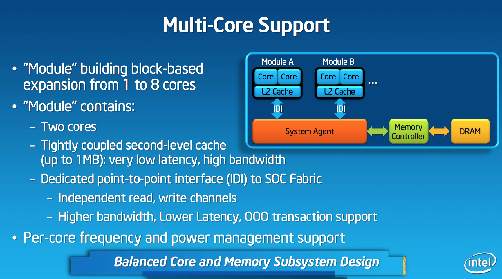
Each module features a shared 1MB L2 cache, a 2x increase over the core:cache ratio of existing Atom based processors. Despite the larger L2, access latency is reduced by 2 clocks. The default module size gives you clear indication as to where Intel saw Silvermont being most useful. At the time of its inception, I doubt Intel anticipated such a quick shift to quad-core smartphones otherwise it might’ve considered a larger default module size.
L1 cache sizes/latencies haven’t changed. Each Silvermont core features a 32KB L1 data cache and 24KB L1 instruction cache.
Silvermont Supports Independent Core Frequencies: Vindication for Qualcomm?
In all Intel Core based microprocessors, all cores are tied to the same frequency - those that aren’t in use are simply shut off (power gated) to save power. Qualcomm’s multi-core architecture has always supported independent frequency planes for all CPUs in the SoC, something that Intel has always insisted was a bad idea. In a strange turn of events, Intel joins Qualcomm in offering the ability to run each core in a Silvermont module at its own independent frequency. You could have one Silvermont core running at 2.4GHz and another one running at 1.2GHz. Unlike Qualcomm’s implementation, Silvermont’s independent frequency planes are optional. In a split frequency case, the shared L2 cache always runs at the higher of the two frequencies. Intel believes the flexibility might be useful in some low cost Silvermont implementations where the OS actively uses core pinning to keep threads parked on specific cores. I doubt we’ll see this on most tablet or smartphone implementations of the design.
From FSB to IDI
Atom and all of its derivatives have a nasty secret: they never really got any latency benefits from integrating a memory controller on die. The first implementation of Atom was a 3-chip solution, with the memory controller contained within the North Bridge. The CPU talked to the North Bridge via a low power Front Side Bus implementation. This setup should sound familiar to anyone who remembers Intel architectures from the late 90s up to the mid 2000s. In pursuit of integration, Intel eventually brought the memory controller and graphics onto a single die. Historically, bringing the memory controller onto the same die as the CPU came with a nice reduction in access latency - unfortunately Atom never enjoyed this. The reasoning? Atom never ditched the FSB interface.
Even though Atom integrated a memory controller, the design logically looked like it did before. Integration only saved Intel space and power, it never granted it any performance. I suspect Intel did this to keep costs down. I noticed the problem years ago but completely forgot about it since it’s been so long. Thankfully, with Silvermont the FSB interface is completely gone.
Silvermont instead integrates the same in-die interconnect (IDI) that is used in the big Core based processors. Intel’s IDI is a lightweight point to point interface that’s far lower overhead than the old FSB architecture. The move to IDI and the changes to the system fabric are enough to improve single threaded performance by low double digits. The gains are even bigger in heavily threaded scenarios.
Another benefit of moving away from a very old FSB to IDI is increased flexibility in how Silvermont can clock up/down. Previously there were fixed FSB:CPU ratios that had to be maintained at all times, which meant the FSB had to be lowered significantly when the CPU was running at very low frequencies. In Silvermont, the IDI and CPU frequencies are largely decoupled - enabling good bandwidth out of the cores even at low frequency levels.
The System Agent
Silvermont gains an updated system agent (read: North Bridge) that’s much better at allowing access to main memory. In all previous generation Atom architectures, virtually all memory accesses had to happen in-order (Clover Trail had some minor OoO improvements here). Silvermont’s system agent now allows reordering of memory requests coming in from all consumers/producers (e.g. CPU cores, GPU, etc...) to optimize for performance and quality of service (e.g. ensuring graphics demands on memory can regularly pre-empt CPU requests when necessary).


174 Comments
View All Comments
xTRICKYxx - Tuesday, May 7, 2013 - link
You're right. Intel has nothing to show at all.... Its not like they have the most powerful mobile and desktop consumer processors available.R0H1T - Tuesday, May 7, 2013 - link
Yeah, now sit & watch that market(x86) die a slow death at the hands of mobile/tablets that are powered by "good enough" ARM which doesn't need teraflop level of performance to sell their stuff unlike Intel !misaki - Monday, May 6, 2013 - link
Wow, clearly you are a new reader. This is an architecture overview, not a performance article, which means the information HAS to come from Intel. They have done these type of articles with every architecture redesign since the 90's.When chips are available to test that is when the real world performance articles will come out.
Ortanon - Monday, May 6, 2013 - link
SERIOUSLY.kyuu - Monday, May 6, 2013 - link
Yes, but a lot of performance claims are being made in the article, and Anand really seemed to just be taking Intel's marketing speak for gospel. That's how it read, at least.xTRICKYxx - Tuesday, May 7, 2013 - link
Not really. He clearly states to take the graphs cautiously. Also Intel may be slightly misleading, but nothing in the graphs are lies. They chose the best possible scenario for the greatest advantage.R0H1T - Tuesday, May 7, 2013 - link
Like how they(AT) claimed Intel's "SDP" was superior after stress testing an Exynos Octa, yup loved that fairytale !Kevin G - Monday, May 6, 2013 - link
The article mentions that the IDI is similar to internal bus found on the Nehalem and later desktop processor. IDI here is mentioned as a point-to-point interconnect where as everything is linked via a ring bus in recent Core processors. Of course you can loop multipe point-to-point interfaces into a loop but the article's wording allows for other topologies.For example, each Silvermont module could have its down dedicated point-to-point link to the system agent. In Nehalem, the system against logically appears as another hop in the internal ring bus.
Exophase - Monday, May 6, 2013 - link
Small correction:"Remember that with the first version of Atom, Intel enabled the fusion of load-op-store and load-op-execute instructions. Instead of these instruction combinations decoding into three and two micro-ops respectively, they would be fused post-fetch and treated like single operations throughout the entire pipeline."
Atom (the current one anyway) doesn't have instruction (macro-op) fusion. It does handle load + op and load + op + store are one issue down the pipeline but they still came from single instructions that are a natural part of the x86 ISA. While these may be considered fused micro-ops in Intel's other CPUs that terminology doesn't fit Atom.
These operations do need multiple instructions on most more RISCy ISAs like ARM. But the same is true the other way around (notably, 3 address arithmetic). I very much doubt you'll find typical x86 programs only need 2 instructions for every 3 ARM instructions on average, or at least any papers I've seen that measure micro-ops vs instructions on high-end CPUs are nowhere close to 1.5 (and a uop isn't generally more powerful than an ARM instruction, sometimes less when you consider two are needed for a store). But there are lots of other places that caused stalls on Atom that weren't related to decode, that it's easy to see how you could still gain a lot of perf/MHz without increasing it - as Bobcat and Jaguar have shown. All the details here do seem to point to a Bobcat-like design only with a much lower L2 cache latency and branch mispredict penalty which can only help more.
Anand Lal Shimpi - Monday, May 6, 2013 - link
Er you're very correct. Atom doesn't break these instructions down further, they're treated like single ops throughout the pipeline. I've updated the section. Thank you!