Intel's Haswell Architecture Analyzed: Building a New PC and a New Intel
by Anand Lal Shimpi on October 5, 2012 2:45 AM ESTCPU Architecture Improvements: Background
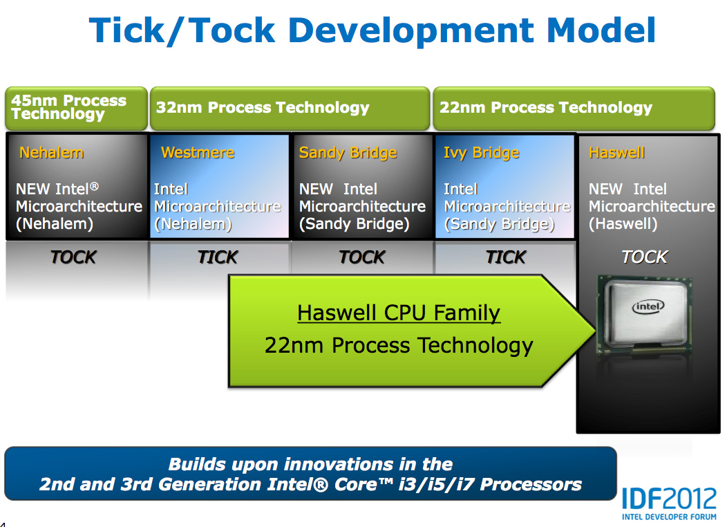
Despite all of this platform discussion, we must not forget that Haswell is the fourth tock since Intel instituted its tick-tock cadence. If you're not familiar with the terminology by now a tock is a "new" microprocessor architecture on an existing manufacturing process. In this case we're talking about Intel's 22nm 3D transistors, that first debuted with Ivy Bridge. Although Haswell is clearly SoC focused, the designs we're talking about today all use Intel's 22nm CPU process - not the 22nm SoC process that has yet to debut for Atom. It's important to not give Intel too much credit on the manufacturing front. While it has a full node advantage over the competition in the PC space, it's currently only shipping a 32nm low power SoC process. Intel may still have a more power efficient process at 32nm than its other competitors in the SoC space, but the full node advantage simply doesn't exist there yet.
Although Haswell is labeled as a new micro-architecture, it borrows heavily from those that came before it. Without going into the full details on how CPUs work I feel like we need a bit of a recap to really appreciate the changes Intel made to Haswell.
At a high level the goal of a CPU is to grab instructions from memory and execute those instructions. All of the tricks and improvements we see from one generation to the next just help to accomplish that goal faster.
The assembly line analogy for a pipelined microprocessor is over used but that's because it is quite accurate. Rather than seeing one instruction worked on at a time, modern processors feature an assembly line of steps that breaks up the grab/execute process to allow for higher throughput.
The basic pipeline is as follows: fetch, decode, execute, commit to memory. You first fetch the next instruction from memory (there's a counter and pointer that tells the CPU where to find the next instruction). You then decode that instruction into an internally understood format (this is key to enabling backwards compatibility). Next you execute the instruction (this stage, like most here, is split up into fetching data needed by the instruction among other things). Finally you commit the results of that instruction to memory and start the process over again.
Modern CPU pipelines feature many more stages than what I've outlined here. Conroe featured a 14 stage integer pipeline, Nehalem increased that to 16 stages, while Sandy Bridge saw a shift to a 14 - 19 stage pipeline (depending on hit/miss in the decoded uop cache).
The front end is responsible for fetching and decoding instructions, while the back end deals with executing them. The division between the two halves of the CPU pipeline also separates the part of the pipeline that must execute in order from the part that can execute out of order. Instructions have to be fetched and completed in program order (can't click Print until you click File first), but they can be executed in any order possible so long as the result is correct.
Why would you want to execute instructions out of order? It turns out that many instructions are either dependent on one another (e.g. C=A+B followed by E=C+D) or they need data that's not immediately available and has to be fetched from main memory (a process that can take hundreds of cycles, or an eternity in the eyes of the processor). Being able to reorder instructions before they're executed allows the processor to keep doing work rather than just sitting around waiting.
Sidebar on Performance Modeling
Microprocessor design is one giant balancing act. You model application performance and build the best architecture you can in a given die area for those applications. Tradeoffs are inevitably made as designers are bound by power, area and schedule constraints. You do the best you can this generation and try to get the low hanging fruit next time.
Performance modeling includes current applications of value, future algorithms that you expect to matter when the chip ships as well as insight from key software developers (if Apple and Microsoft tell you that they'll be doing a lot of realistic fur rendering in 4 years, you better make sure your chip is good at what they plan on doing). Obviously you can't predict everything that will happen, so you continue to model and test as new applications and workloads emerge. You feed that data back into the design loop and it continues to influence architectures down the road.
During all of this modeling, even once a design is done, you begin to notice bottlenecks in your design in various workloads. Perhaps you notice that your L1 cache is too small for some newer workloads, or that for a bunch of popular games you're seeing a memory access pattern that your prefetchers don't do a good job of predicting. More fundamentally, maybe you notice that you're decode bound more often than you'd like - or alternatively that you need more integer ALUs or FP hardware. You take this data and feed it back to the team(s) working on future architectures.
The folks working on future architectures then prioritize the wish list and work on including what they can.


245 Comments
View All Comments
FunBunny2 - Friday, October 5, 2012 - link
While not a hardware issue (and thus not an AnandTech major venue), I would be amused if one of your writers explored the implications on data storage design (normal form databases vs. traditional files) of small real estate mobile. My take is that small, consistent bites of bytes are required, and will eventually change how data is stored on the servers. Any takers?lukarak - Saturday, October 6, 2012 - link
In other words, "....all cars were trucks....."?BoloMKXXVIII - Friday, October 5, 2012 - link
Very well written article. Other sites should read Anandtech to see how it should be done.Thank you.
All this power saving in idle conditions is great (love the looping of frame buffer idea), but users aren't always reading text on their screens. When these chips are under load they are still going to draw very significant amounts of power. Unless battery technology improves by an order of magnatude I don't see Haswell (or its replacements) fitting into ultraportable devices like phones or "phablets". The other comments concerning AMD are on the mark. AMD is in big trouble. They are too far behind Intel right now and every indication is they will be falling further behind.
silverblue - Friday, October 5, 2012 - link
Steamroller will haul AMD back towards Intel. Not completely, but a lot closer than they have been, and potentially even ahead in some cases. Still, that process deficit has to be painful, as AMD can only win on idle power.I really hope GF don't mess up again, as delays really are costing AMD dearly. Steamroller is a good design, the sort that means AMD can have a cheaper but still decent part, but I fear it'll come too late.
Intel CPUs are looking even more tasty than ever.
overseer - Friday, October 5, 2012 - link
Great Article.Then I sincerely hope AMD can still survive and stride forward in this mobile tide. (R.R. and J.K., you reading this?)
It may look silly but I do like underdogs and their (solid) products, especially when they achieved something with less talents, capital and executiveness.
wumpus - Friday, October 5, 2012 - link
"To put it in perspective, you'll be able to get something faster than an Ivy Bridge Ultrabook or MacBook Air, in something the size of your smartphone, in fewer than 8 years". I can tell you right now, while this architecture is absolutely great on a motherboard, this isn't the right path to the mobile space."Haswell is the first step of a long term solution to the ARM problem." Unfortunately, anandtech is one of the few places left that can call intel on this marketing blather. Intel's ARM problem is that there is no more efficient way to execute instructions than on a in-order, single instruction issue, clean RISC design: all of which are standard features on an ARM. ARM's intel problem is that this limits you to about .5GIPS ([G]meanless indicator of processor speed) compared to over 6GIPS on an all out Intel design.
The choice isn't all or nothing, just that this time Intel choose performance over efficiency. MIPS, alpha, (to a large part) PowerPC all fell to high performance Intel chips that were vastly less complex than current designs. ARM could try to compete with Intel on performance, but if they are lucky they will end up like AMD, and if they can't out design Intel (remember Intel's process advantage) they will end up like MIPS, etc.
The reason this all appears to be built around speed (and not efficiency) can be found on pages 7 and 8 (despite protests listed on those pages). Intel needs to add wider execution paths to try to get a tiny few more instructions out per second, all the while holding even more (than ivy or sandy) instructions in flight in case it can execute one. All this means a much longer path for any instruction and many more things computed, more leaky transistors leaking picoamps, more latches burning nanowatts. All ARM has to do is execute one after another.
I am surprised that they bothered to toot their horn about the GPU. It might beat ARM, but any code that can be made to fit a GPU should be run on an AMD machine (or possibly discrete nVidia board). They have been pushing Intel graphics for at least 15 years, don't pretend they are ever going to get it right.
In conclusion, I want one of these in my desktop. A phone CPU should look much more like an early core (maybe core2) design, maybe even more like a pentium pro.
A5 - Friday, October 5, 2012 - link
If we're going to start a RISC/CISC battle, you should really look at a modern ARM architecture before talking.What you can fit in a phone today isn't going to be what you can fit in a phone 8 years from now (in terms of both TDP and die size).
Getting Haswell-class performance from a 2020 smartphone isn't that far-fetched...you can argue that modern smartphone SoCs are close to the performance of the Athlon 64 2800+ or the Prescott Pentium 4s of 2004 in a lot of tasks.
wumpus - Friday, October 5, 2012 - link
There is a reason Atom is getting creamed in the phone space by ARM. Also the only way TDP is going to change is with major increases in battery technology. X Joules (typically changed to W/hr in battery speak, but why not stick with SI units) means X seconds a 1 W or X/n seconds at n Watts.On the high end, everything that won the war for CISC (namely, Intel's manufacturing skills) is even more true than when they won. There isn't going to be another. That doesn't mean that a chip designed for all out performance is going to have any business competing with ARM on MIP/W. If they wanted to compete on battery life, they would have scaled down the depth and breadth of the queue, not increased it.
Actually, I was ready to go into full rant when I saw the opening. Then I checked that "ultrabook" meant 1.8GHz i3s. It is quite possible (although I still doubt it is a good way to use a battery) to build a chip that will do that and have low power. I just don't think that Haskel is anyway designed to be that chip
FunBunny2 - Friday, October 5, 2012 - link
-- everything that won the war for CISC (namely, Intel's manufacturing skills) is even more true than when they wonIt's been true since P4 that the "real" cpu is a RISC engine fronted by a x86 ISA translator. Intel tried to sell a ISA level RISC chip (twice). Not so hot. But Intel does know RISC. I've always wondered why they used all that transistor budget the way they did, rather than doing the entire instruction set in hardware, as they could have. It's as if IBM turned all the 370s into 360/30s.
Penti - Saturday, October 6, 2012 - link
It was Pentium Pro that switched to a modern out of order micro-ops powered CPU. I.e. P6. It's only the front end that speaks x86. Intel's own RISC designs like i960 ultimately failed and EPIC even more so when it failed to outdo AMD and Intel server processors in enterprise applications. In reality customers only switched to Itanium because they already had made up their mind before there even was any product thus killing at the time more appropriate Alpha, MIPS and PA-RISC processors. But as soon as those where fased out, Intel's x86 compatible chips had already gained the enterprise features that it missed previously and that set those older chips apart.The front end and x86 decode doesn't use that much space in modern processors at all. CPU architecture aren't really all that important it's today largely about the features it supports, the gpu, video decode/processor etc. ARM just made it into the out-of-order superscalar era in 2011 with A9, superscalar in-order in 2008 with Cortex A8. Atom is kinda designed like a P5 cpu. I.e. superscalar in-order, and moves to an out-of-order design next year. Intel's first superscalar design was in 1988.
ARM just needs to be fast enough, it was fairly easy to replace SH3, Motorola DragonBall, i386 design in the mobile space it was even Intel that did it to a large part. And earlier 8086-stuff had already been left behind by that time. Now what's impressive is the integration and finish of the ARM SoC's. It was Intel that didn't want companies like Research In Motion to continue use low-power Intel x86-chips in their handheld devices. That only changes when Intel sold off the StrongARM/XScale line in 2006. Intel has no reason to start create custom ARM ISA chips again as they can compete with them with x86 chips which they spend much larger time to adapt development tools and frameworks for any way. Atom as a whole has a much larger market then XScale had on it's own. Remember that Intel dropped stuff like RAID/Storage-processors too. Having Intel as a Marvell in ARM chips today wouldn't have changed anything radically.