Intel's Haswell Architecture Analyzed: Building a New PC and a New Intel
by Anand Lal Shimpi on October 5, 2012 2:45 AM ESTOther Power Savings
Haswell's power savings come from three sources, all of which are equally important. We already went over the most unique: Intel's focus on reducing total platform power consumption by paying attention to everything else on the motherboard (third party controllers, voltage regulation, etc...). The other two sources of power savings are more traditional, but still very significant.
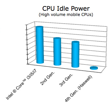
At the micro-architecture level Intel added more power gating and low power modes to Haswell. The additional power gating gives the power control unit (PCU) more fine grained control over shutting off parts of the core that aren't used. Intel published a relatively meaningless graph showing idle power for standard voltage mobile Haswell compared to the previous three generations of Core processors.
Haswell can also transition between power states approximately 25% faster than Ivy Bridge, which lets the PCU be a bit more aggressive in which power state it selects since the penalty of coming out of it is appreciably lower. It's important to put the timing of all of this in perspective. Putting the CPU cores to sleep and removing voltage/power from them even for a matter of milliseconds adds up to the sort of savings necessary to really enable the sort of always-on, always-connected behavior Haswell based systems are expected to deliver.
Intel has also done a lot of work at the process level to bring Haswell's power consumption down. As a tock, Haswell is the second micro-architecture to use Intel's new 22nm tri-gate transistors. The learnings from Ivy Bridge are thus all poured into Haswell. Intel wasn't too specific on what it did on the manufacturing side to help drive power down in Haswell other than to say that a non-insignificant amount of work came from the fabs.
The Fourth Haswell
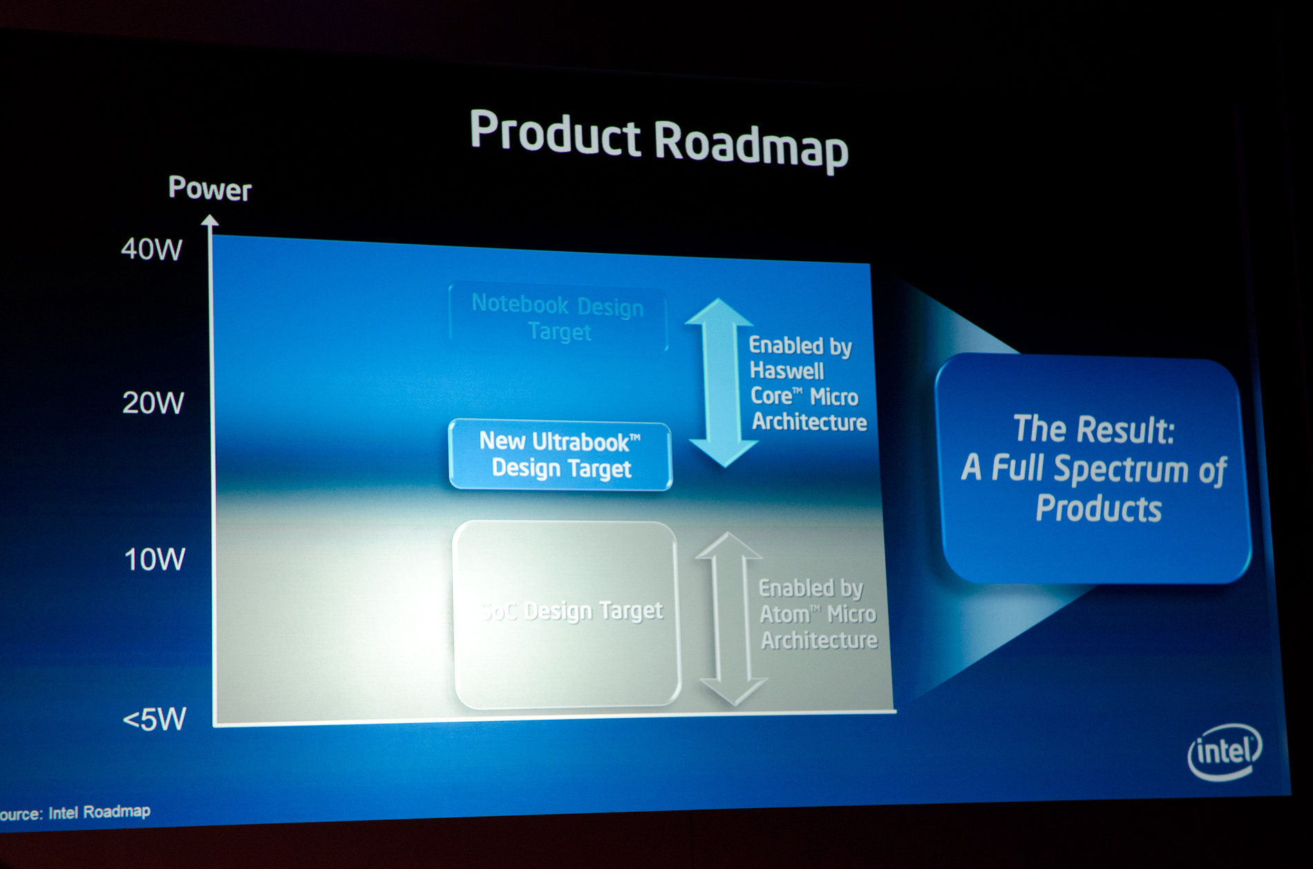
At Computex Intel's Mooly Eden showed off this slide that positioned Haswell as a 15-20W part, while Atom based SoCs would scale up to 10W and perhaps beyond:
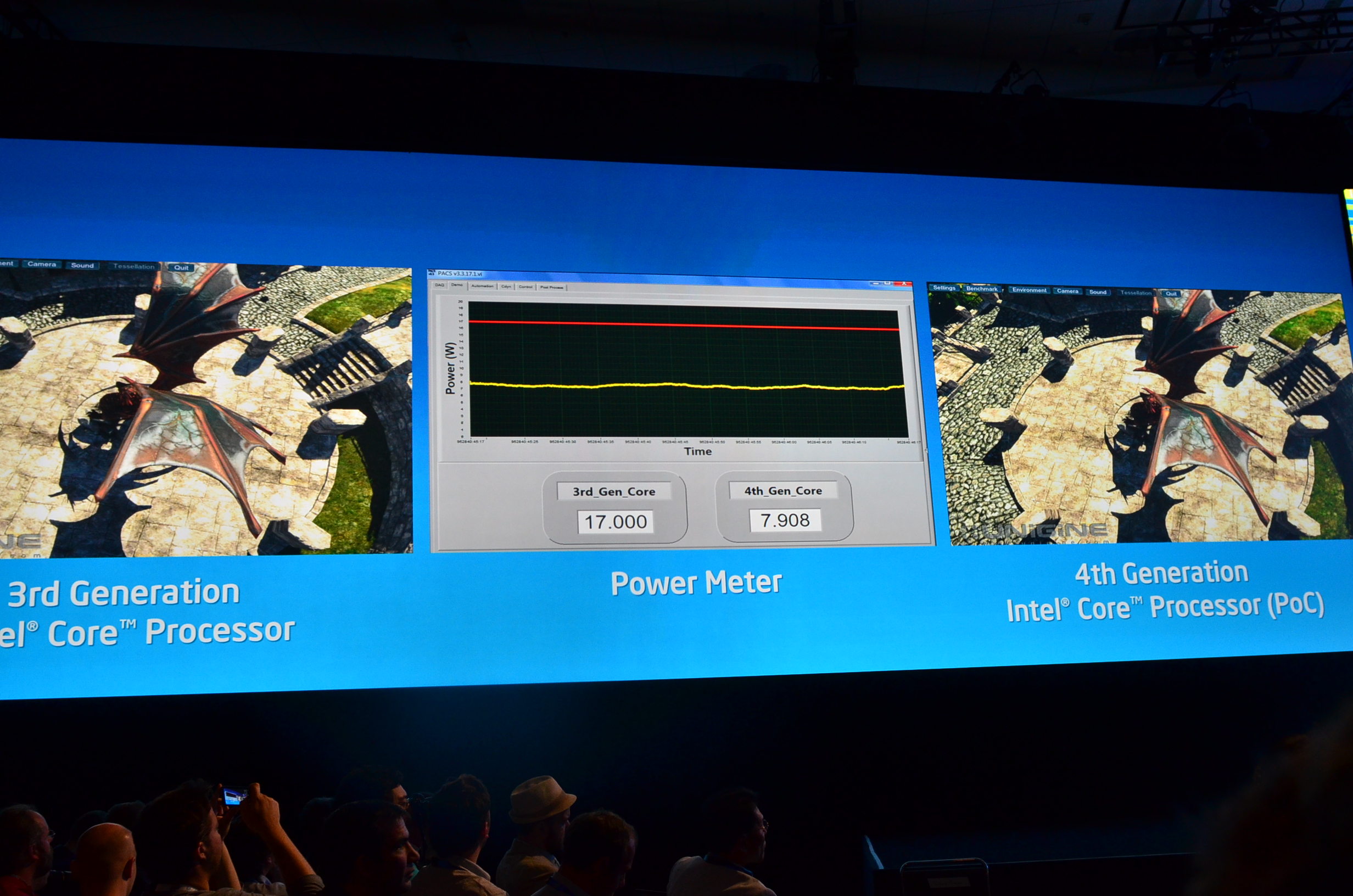
Just before this year's IDF Intel claimed that Haswell ULT would start at 10W, down from 17W in Sandy/Ivy Bridge. Finally, at IDF Intel showed a demo of Haswell running the Unigen Heaven benchmark at under 8W:
The chain of events tells us two things: 1) Intel likes to play its cards close to its chest, and 2) the sub-10W space won't be serviced by Atom exclusively.
Intel said Haswell can scale below 10W, but it didn't provide a lower bound. It's too much to assume Haswell would go into a phone, but once you get to the 8W point and look south you open yourself up to fitting into things the size of a third generation iPad. Move to 14nm, 10nm and beyond then it becomes more feasible that you could fit this class of architecture into something even more portable.
Intel is being very tight lipped about the fourth client Haswell (remember the first three were desktop, mobile and ultra-low-volt/Ultrabook) but it's clear that it has real aspirations to use it in a space traditionally reserved for ARM or Atom SoCs.
One of the first things I ever heard about Haswell was that it was Intel's solution to the ARM problem. I don't believe a 10W notebook is going to do anything to the ARM problem, but a sub-8W Haswell in an iPad 3 form factor could be very compelling. Haswell won't be fanless, but Broadwell (14nm) could be. And that could be a real solution to the ARM problem, at least outside of a phone.
As I said before, I don't see Haswell making it into a phone but that's not to say a future derivative on a lower power process wouldn't.


245 Comments
View All Comments
kukreknecmi - Friday, October 5, 2012 - link
I hope i know it right. L3 on SB/IB doest used by GPU. L3 still servers as cache on system via memory controller. If GPU nneds to acess to memory, it sends request to memory controller. L3 is not directly accessable to GPU as a texture cache etc.On IB, they added a 512k cache which is seperated to half, 256k of it is used as texture system as backfeeding and other 256k half is used for other things.Article implies that L3 cache on IB is used as a texture buffer like on ordinary graphic cards. Only on Haswell L3 cache will be accessable and can be used as a some kind of GPU specific buffer.
Kevin G - Friday, October 5, 2012 - link
The confusing thing is that consumer Ivy Bridge parts have a L3 cache just for the GPU which is separate memory than the L3 cache that the CPU uses. The Ivy Bridge GPU's can use the CPU's L3 cache as the GPU's L4 cache to a degree.To confuse things further, the CPU side really has four levels of cache too. There is the small 1.5 KB micro-uop cache for instructions which comes before the 32 KB L1 instruction cache.
mayankleoboy1 - Friday, October 5, 2012 - link
From the article, its not very clear : Which platform (DT, Mobile, ultra mobile) will have the integrated voltage regulators/controllers ?Ryan Smith - Friday, October 5, 2012 - link
Ultra Mobile.Anand Lal Shimpi - Friday, October 5, 2012 - link
It's not clear how much of the VR circuitry gets integrated into Haswell or necessarily which parts will have it and which ones won't. Ultra mobile is a shoe in, but I've even heard of desktop parts getting it as well. We'll have to wait and see.DanNeely - Friday, October 5, 2012 - link
Rats. Reading the article I was hoping that Intel had decided to only bake the VRMs into their ultra-mobile parts. Better VRMs are an important factor in high end OCing; with desktop boards not cramped for space I really hope Intel keeps them off the package.Peanutsrevenge - Friday, October 5, 2012 - link
Seconded.However, I wonder whether the VRMs on high end mobos will still be an option, where the on package VRMs will simply extend the capabilities?
But given Intels recent distaste for overclocking, it wouldn't suprise me if we'll soon see CPUs completely locked from overclocking completely or only on E series, high profit chips.
Homeles - Saturday, October 6, 2012 - link
"However, I wonder whether the VRMs on high end mobos will still be an option, where the on package VRMs will simply extend the capabilities?"Bingo.
Homeles - Saturday, October 6, 2012 - link
Low end motherboards won't need them. High end overclocking boards will have them in addition to the ones on package.tuxRoller - Friday, October 5, 2012 - link
Using lvds reclocking you can reduce idle screen induced wakeups to 30 (ditto for the memory controller if the cpu supports self refresh for the sram ).eDP may allow even less.